LVDS Output with 600 mV to 1200 mV Output Swing
Contents
1. Introduction
2. LVDS Output Principles of Operation
3. Adjusting LVDS Differential Swing to 600 mV to 1200 mV
1. Introduction
A reference clock output with a differential swing of 600 mV to 1200 mV as defined in Figure 1.1 below is becoming a common requirement for optical modules and is driven by the chipset input requirements. This definition of differential swing is defined as OUT+ minus OUT- and is how the differential receiver will process the waveform. The OUT+ minus OUT- subtraction effectively doubles the amplitude of waveform relative to an oscilloscope observation when measuring each of the differential outputs in single-ended mode as shown in Figure 1.2 on page 2 for example purposes. Because different differential output formats can have different definitions for differential waveform swing levels, it is very important to confirm the exact requirements with the chipset vendor, preferably with a waveform diagram.
This application note discusses use of the SiTime SiT9365/SiT9366 LVDS output to provide 600 mV to 1200 mV differential swing amplitude as defined in Figure 1.1 below.
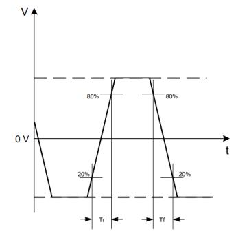
Figure 1.1. Differential Waveform Definition
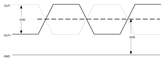
Figure 1.2. Differential Output ‒ Single-Ended View
2. LVDS Output Principles of Operation
LVDS is a high-speed digital interface suitable for many applications that require low power consumption and high noise immunity. LVDS outputs use differential signals with low voltage swings to transmit data at high rates. on the following page shows the output structure of an LVDS driver, consisting of 3.5 mA nominal current sources connected to differential outputs via a switching network, sometimes referred to as “H” switch. The outputs are typically connecting to 100 Ω differential transmission lines terminated with a 100 Ω resistor across the receiver inputs. The resistor value matches the impedance of the transmission lines and provides a current path for the signal.
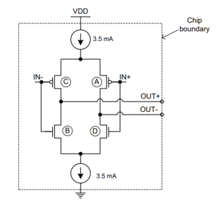
Figure 2.1. LVDS Driver Output Structure
The driver includes circuitry to set the common mode to 1.2 V nominally regardless of VDD. Therefore, there is no need for externally biasing the driver to any specific voltage. Also, an LVDS output can be connected to any LVDS input without any concern about actual supply voltage of the oscillator.
Signal switching is accomplished with four transistors labeled A, B, C, and D. Since the impedance of the receiver is typically high, virtually all current from the driver flows through the standard 100 Ω differential termination resistor, resulting in a voltage difference of 350 mV between the receiver inputs. In Figure 2.1, when the signal IN is low, transistors A and B are turned on; the current flows through the transistor A and the 100 Ω resistor and returns through the transistor B. When the signal IN is high, transistors C and D are turned on; the current flows through the transistor C and the 100 Ω resistor and returns through the transistor D, resulting in -350 mV voltage across the receiver. From the receiver’s perspective, the direction of the current flowing through the termination resistor determines whether a positive or negative differential voltage is registered. A positive differential voltage represents a logic high level, while a negative differential voltage represents a logic low level.
3. Adjusting LVDS Differential Swing to 600 mV to 1200 mV
Differential output swing of SiTime oscillators with LVDS output and standard 100 Ω termination is 700 mV typical with 500 mV to 900 mV minimum-to-maximum window. To adjust the differential LVDS swing to the 600 mV to 1200 mV range, SiTime recommends a termination resistor value of 130 Ω as shown in figure 3.0 below. It will move typical output swing value to 910 mV and minimum-to-maximum range to 650 mV to 1170 mV. To get full impedance matching of the transmission line and termination resistor, it is recommended to increase line impedance to 65 Ω.
If an LVDS driver and receiver are operating with different common mode voltages, an AC termination is recommended. A capacitor is used to block the DC current path from the driver, so the receiver must implement its own input bias circuit. AC coupling termination circuit is shown at Figure 3.1 and Figure 3.2. As shown on these termination diagrams, the AC-coupling capacitors can be placed before or after the load termination resistor.
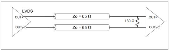
Figure 3.1. LVDS Single AC Termination at the Load
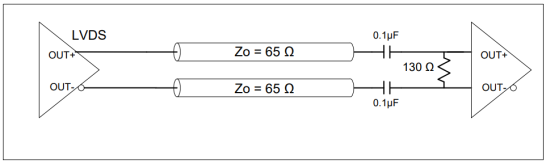
Figure 3.2. LVDS Single AC Termination at the Load
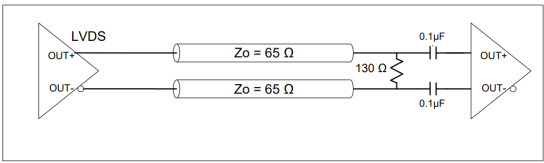
Figure 3.3. LVDS Single AC Termination at the Load