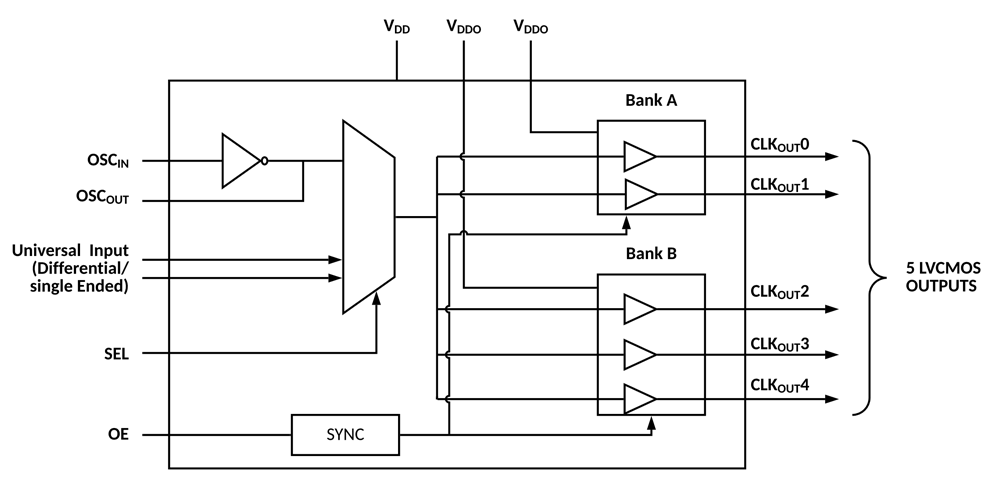
The SiT92113 is a 5-output, low-jitter fanout clock buffer. It is ideal for low-jitter, high-frequency clock/data distribution. The low impedance LVCMOS outputs are designed to drive 50 Ω series or parallel terminated transmission lines.
The buffer can use a clock input from primary or secondary clock sources, either single ended or fully differential. The selected clock is distributed to 5 LVCMOS output drivers.
The SiT92113 operates from a 3.3 V/2.5 V core supply and 3.3 V/2.5 V output supply. The core supply and output supply are independent of each other and no supply sequencing is required.

| "Specs" | "Value" |
|---|---|
| Operating Temperature Range (°C) | -40 to 85 |
| Package Type (mm²) | 4x4 mm, 24-pin QFN |
| Buffer Type | Fanout |
| Number of Inputs | 1 |
| Number of Outputs | 5 Single Ended |
| Input Type | LVPECL, LVDS, LVCMOS, SSTL, HCSL |
| Input Frequency Range | 0 Hz to 250 MHz |
| Output Type | LVCMOS |
| Output Frequency Range | 0 Hz to 250 MHz |
| Additive Phase Jitter (rms) | 50 fs |
| Propagation Delay, Typical | 1.4 ns |
| Output-Output Skew, Typical | 30 ps |
| Availability | Production |
-

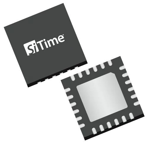
4x4 mm, 24-pin QFN Clock Buffer package
- Level translation with core supply voltage of 3.3 V/2.5 V and 3.3 V/2.5 V / 1.8 V/ 1.5 V output supply for LVCMOS output drivers.
- The inputs are selected by programming input select pins of SiT92113. The input clock receiver in SiT92113 can accept LVPECL, LVDS, LVCMOS, SSTL, HCSL and OSC waveforms.

- Ethernet
- 5G Infrastructure
- Wireless Equipment
- Small Cells
SiT92113 Evaluation Board HW User Manual – Configure and evaluate device performance
Apply Filters
| Resource Name | Resource Type | Date | Format | Size |
|---|
