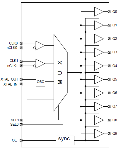
The SiT92110 is a 10-output, low-jitter fanout clock buffer. It is ideal for low jitter, high-frequency clock/data distribution. The low impedance LVCMOS outputs are designed to drive 50 Ω series or parallel terminated transmission lines.
The buffer can use a clock input from primary or secondary clock sources, either single ended or fully differential. The selected clock is distributed to 10 LVCMOS output drivers.
The SiT92110 operates from a 3.3 V/2.5 V/1.8 V core supply and 3.3 V/2.5 V/1.8 V/1.5 V output supply. The core supply and output supply are independent of each other and no supply sequencing is required.

Don’t waste time shipping samples. Request demo & test parts remotely in our lab and qualify for your design today.
We are ready to help you!
Please complete the form below and someone will contact you. Items notated with an * are required.
| "Specs" | "Value" |
|---|---|
| Operating Temperature Range (°C) | -40 to 85 |
| Package Type (mm²) | 5x5 mm, 32-pin QFN |
| Buffer Type | Fanout |
| Number of Inputs | 1 |
| Number of Outputs | 10 Single Ended |
| Input Type | LVPECL, LVDS, LVCMOS, SSTL, HCSL |
| Input Frequency Range | 0 Hz to 250 MHz |
| Output Type | LVCMOS |
| Output Frequency Range | 0 Hz to 250 MHz |
| Additive Phase Jitter (rms) | 50 fs |
| Propagation Delay, Typical | 1.4 ns |
| Output-Output Skew, Typical | 30 ps |
| Availability | Production |
-

5x5 mm, 32-pin QFN Clock Buffer package
- Level translation with core supply voltage of 3.3 V/2.5 V/1.8 V and 3.3 V/2.5 V/1.8 V/1.5 V output supply for LVCMOS output drivers.
- The inputs are selected by programming input select pins of SiT92110. The input clock receiver in SiT92110 can accept LVPECL, LVDS, LVCMOS, SSTL, HCSL and OSC waveforms.
SiT92110 Evaluation Board HW User Manual – Configure and evaluate device performance
| Resource Name | Resource Type | Date | Format | Size |
|---|