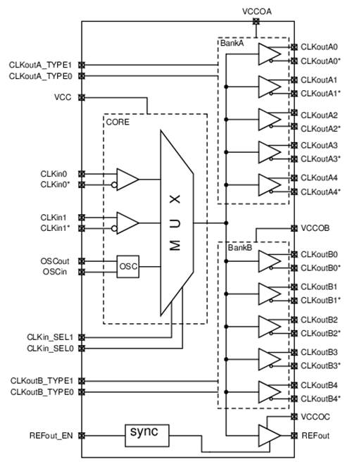
The SiT92211 is a 10-output, low-jitter fanout clock buffer that supports frequencies up to 2.1 GHz. It is ideal for low-jitter, high-frequency clock/data distribution and level translation applications.
The buffer can use a clock input from primary or secondary clock sources, either single ended or fully differential. The selected clock can be distributed to two output drive banks A, B and one LVCMOS output.
The output drivers of each bank can be independently programmed to LVPECL, LVDS, HCSL or HIZ mode. The LVCMOS clock output is synchronized to selected clock and can be enabled or disabled in a glitch free manner.
The SiT92211 operates from a 3.3 V/2.5 V core supply and 3 independent 3.3 V/2.5 V output supplies. The LVCMOS output driver can operate at 1.8 V.

Don’t waste time shipping samples. Request demo & test parts remotely in our lab and qualify for your design today.
We are ready to help you!
Please complete the form below and someone will contact you. Items notated with an * are required.
| "Specs" | "Value" |
|---|---|
| Operating Temperature Range (°C) | -40 to 85 |
| Package Type (mm²) | 7x7 mm, 48-pin QFN |
| Buffer Type | Fanout |
| Number of Inputs | 1 |
| Number of Outputs | 10 Differential |
| Input Type | LVPECL, LVDS, LVCMOS, SSTL, HCSL |
| Input Frequency Range | 0 Hz to 2.1 GHz |
| Output Type | LVPECL, LVDS, HCSL, LVCMOS |
| Output Frequency Range | 0 Hz to 2.1 GHz |
| Additive Phase Jitter (rms) | 55 fs |
| Propagation Delay, Typical | 1.4 ns |
| Output-Output Skew, Typical | 30 ps |
| Availability | Production |
-

7x7 mm, 48-pin QFN Clock Buffer package
- 3:1 input clock selection.
- Two universal clock inputs can operate up to 2.1 GHz and accept LVPECL, LVDS, LVCMOS, CML(ac-coupled only), HCSL, SSTL or single ended clocks.
- Two output driver banks A and B which can be programmed independently to LVPECL, LVDS, HCSL or HIZ mode.
- Level translation with core supply voltage of 3.3 V/2.5 V and 3.3 V/2.5 V output supply for differential output drivers.
- 3.3 V/2.5 V/1.8 V operation for the single LVCMOS output driver.
- High PSRR -70/-73 dBc for LVPECL/LVDS modes.
- Supports PCI-e Gen 1 to Gen 5.
SiT92211 Evaluation Board HW User Manual – Configure and evaluate device performance
| Resource Name | Resource Type | Date | Format | Size |
|---|