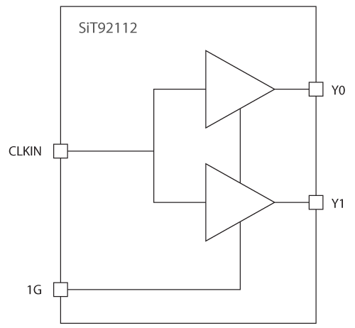
The SiT92112 is a high-performance LVCMOS fanout clock buffer with additive phase jitter of only 50 fs RMS.
The SiT92112 supports a synchronous glitch-free output enable (OE) function to eliminate any potential intermediate incorrect output clock cycles when enabling or disabling outputs. It can operate from a 1.8 V to 3.3 V supply.

| "Specs" | "Value" |
|---|---|
| Operating Temperature Range (°C) | -40 to 85 |
| Package Type (mm²) | 2x2 mm, 8-pin DFN |
| Buffer Type | Fanout |
| Number of Inputs | 1 |
| Number of Outputs | 2 Single Ended |
| Input Type | LVCMOS |
| Input Frequency Range | 0 Hz to 200 MHz |
| Output Type | LVCMOS |
| Output Frequency Range | 0 Hz to 200 MHz |
| Additive Phase Jitter (rms) | 50 fs |
| Propagation Delay, Typical | 1.0 ns |
| Output-Output Skew, Typical | 50 ps |
| Output Enable | Yes |
| Availability | Production |
-

2x2 mm, 8-pin DFN Clock Buffer package
- High-performance 1:2 Buffer.
- LVCMOS clock buffer.
- Very low pin-to-pin skew: <50 ps.
- Very low additive jitter: <50 fs.
- Supply voltage: 1.8 V to 3.3 V.
- 3.3 V tolerant input clock.
- FMAX = 200 MHz.
- Integrated serial termination for 50 Ω channel.
- Packaged in 8 pin, 2 x 2 mm DFN packages.

SiT92112 Evaluation Board HW User Manual – Configure and evaluate device performance
Apply Filters
| Resource Name | Resource Type | Date | Format | Size |
|---|
