Contents
4. Power supply noise reduction
5. Layout recommendations for SiTime clocks
5.1 Recommendation for single-ended clocks
5.2 Recommendation for differential-ended clocks
5.3 Transmission line impedance calculation
5.4 1508 CSP and 2012 QFN package layout
5.4.1 Solder printing stencil recommendations for 1508 CSP
5.5 SiTime specific package layout example
5.5.1 SiTime 5032 ceramic package layout
5.5.2 SiTime OCXO 7 x 9 mm package layout
1. Introduction
This application note provides guidelines for printed circuit board (PCB) designs that incorporate SiTime oscillators. Good board layout practices are required to achieve the expected performance from SiTime timing devices. These design guidelines help to achieve high quality and reliable results such as low noise levels, signal integrity, impedance matching, power requirements, and solder joint reliability. The guidelines described in this document supplement standard board layout best practices and are based on our experience.
2. General layout techniques
Use a thermal pad for GND and VDD pins. This makes it easier to solder and de-solder the oscillator and avoids creating cold solder joints.
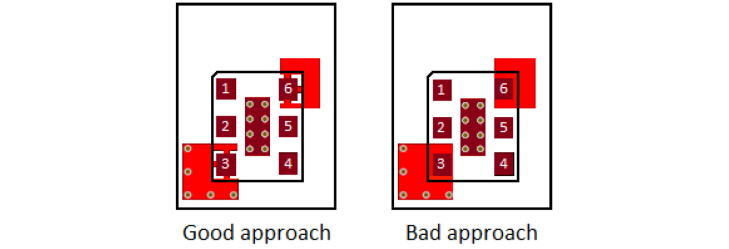
Figure 1: Thermal Pads Use Approaches
- Physically locate the clock source chip as close as possible to the load. Shorter signal paths produce less electromagnetic emissions. Another advantage is that it is typically easier to maintain signal integrity when the clock signal path is shorter.
- Do not use 90-degree angle bends when routing clock signal traces because it affects the clock signal integrity. If a clock trace bend is necessary, use two 45-degree bends (good) or a curved bend (best).
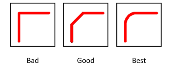
Figure 2: Clock signal trace bend impact
- To lower system EMI and create more EMC-robust designs, avoid routing noise emission (e.g., oscillator clocks) or noise immunity (e.g., VDD lines) critical signals near circuit board edges.
- Trace impedance matching is important for high-speed signals because mismatched impedance can distort such signals. This helps avoid signal integrity issues.
- Avoid routing high-speed traces under the oscillator or high-current, modulated signal circuits (e.g., DC-DC converter output) near the oscillator.
- Use extra clearance between clock traces and adjacent signals (especially high-speed or fast slew-rate signals) to reduce crosstalk. Adding a ground trace or polygon connected on both sides is also helpful to minimize crosstalk.
- When using passive components on the clock traces, try to overlay their pads on the clock trace without any branching and keep their pads the same width as the clock traces.
- In a multi-layer board design, using a ground plane is recommended. Having one layer of the PCB as a continuous ground plane lets each signal have the shortest return path and decreases coupling and interference. A good practice is to place a ground plane under each signal layer to ensure the shortest return path.
- For QFN packages, the stencil aperture opening should be a 1:1 ratio to the metal pad. If the thermal pad of the device is larger than 2 mm X 2 mm, then the stencil aperture may need to be designed as an array of openings instead of one large opening.
3. Decoupling and bypassing
Fast switching outputs of devices such as clock oscillators can be the largest contributor to instantaneous current issues. Decoupling is necessary to prevent instantaneous currents and is only effective when the inductance is minimized. Low inductance decoupling provides localized high-frequency energy to decouple noise from the switching currents of the device power bus. This is most effective when bypass capacitors are in close proximity to the device VDD pin.
Consider the following bypass capacitor placement variants:
- Bypass capacitor is not placed
- Bypass capacitor of 100 nF is placed far from DUT, at C1 location
- Bypass capacitor of 100 nF is placed near DUT, at C2 location
Power is fed to the DUT by the blue wire to imitate the parasitic inductance of the power trace.
The result of the decoupling capacitor placement is shown in the following two figures.
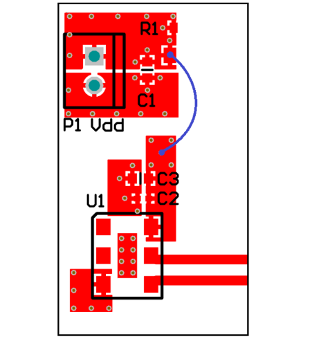
Figure 3: Layout example of decoupling capacitors placement
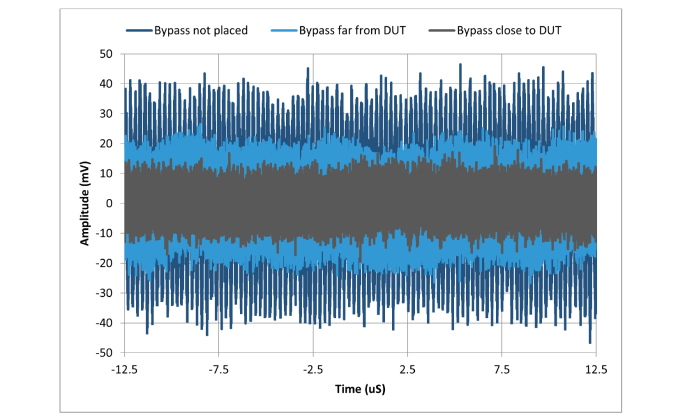
Figure 4: Confirming power supply noise suppression effect, SiT9366-156.25MHz
As can be seen in the figure above, the best approach is to place the bypass capacitor as close as possible to the timing device VDD pin. Excessive power noise can lead to oscillator performance degradation. The figure below shows the SiT9366’s phase noise response with different bypass capacitor placements.
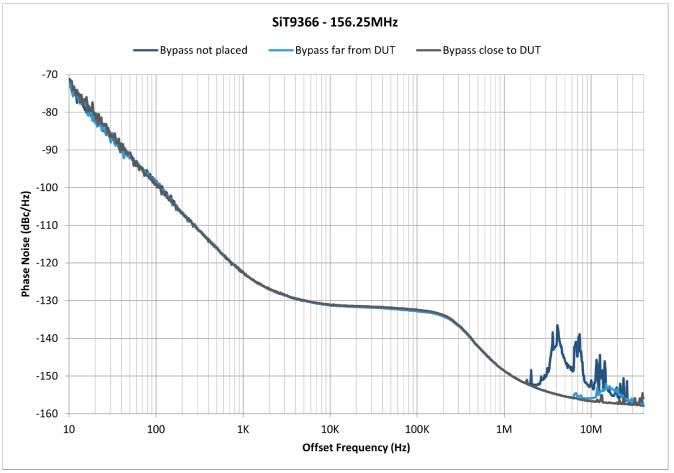
Figure 5: Phase noise response with different bypass capacitor placement for SiT9366-156.25 MHz
The figure above shows how important proper bypass capacitor placement is to achieve the expected oscillator performance.
4 Power supply noise reduction
In most applications, a single 100 nF capacitor between VDD and GND will shunt much of the noise that may exist on the power supply to GND. SiTime devices use an internal regulator to reduce the impact of the power supply noise. However, to further minimize any residual power supply noise impact on the oscillator output jitter, the user may consider RC or LC power supply filtering strategy. SiTime recommends using such filtering for high-speed applications, such as serial interfaces with greater than 6 Gbps baud rates (e.g., 8.5 Gbps Fibre Channel and Serial 10 Gbit Ethernet).
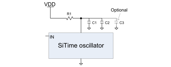
Figure 6: RC power supply filter
RC filtering, shown in the figure above, is simple to use. The R1 value needs to be selected such that the voltage at the VDD input pin is maintained within the specifications described in the datasheet. The table below shows the values for different SiTime oscillators.
Table 1: Recommended component values for RC power supply filter
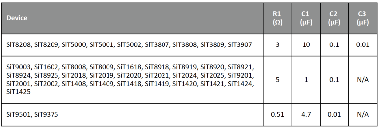
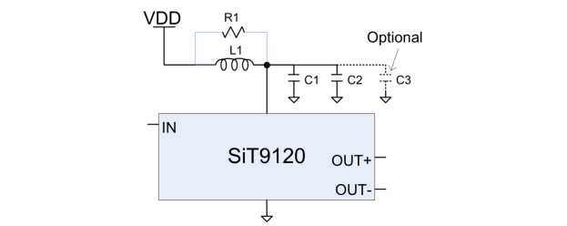
Figure 7: LC power supply filter
LC filtering, shown in the figure above, is particularly suited for devices with higher current consumption, such as differential oscillators. The inductor low series resistance (typically less than 1Ω) delivers the DC supply voltage to the device with less than 50 mV drop. The LC filter has the added advantage of minimizing potential oscillator switching noise coupling to the power network. The resistor in parallel with the inductor is intended to reduce the peaking at the resonance frequency of the LC circuit. The table below lists the recommended component values for LC power supply filters for some of the SiTime devices. A similar filter can also be used with other SiTime differential or single-ended oscillators.
Table 2: Recommended component values for LC power supply filter
5. Layout recommendations for SiTime clocks
5.1 Recommendation for single-ended clocks
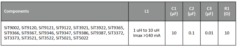
For optimized clock signal routing, it is important to keep the clock traces as short as possible so that the system can be treated as lumped. If that is not possible, the system will be treated as distributed and a clock trace is treated as a transmission line. When the transmission line is considered, it is important to match the line impedance with the output driver impedance of the oscillator. The following table lists the typical driver impedances for various single-ended SiTime oscillators.
Table 3: Typical impedance of various SiTime oscillator output drivers
For calculating trace impedance, refer to the section Transmission line impedance calculation.
In most cases, transmission lines with 50Ω impedance are used, which is optimal in terms of signal energy loss. From the above table, we can see that to match the output driver impedance with the trace impedance, a series termination resistor is required. The best approach is to place the series termination resistor in close proximity to the oscillator/resonator output.
The figure below shows the following different impedance matching conditions:
- Waveform 1 (impedance mismatched 1) – SiT8208 (driver impedance 16 Ω) driving a 50 Ω trace without serial termination
- Waveform 2 (impedance mismatched 2) – SiT8208 (driver impedance 16 Ω) driving a 75 Ω trace without serial termination
- Waveform 3 (impedance matched) – SiT8208 (driver impedance 16 Ω) driving a 50 Ω trace
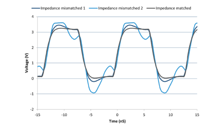
Figure 8: Waveforms measured at load for multiple impedance match conditions, SiT8208 - 75 MHz, 3.3 V
As we can see, two waveforms have over- and under-shoots. This is due to reflections caused by the driver-totrace mismatch. Such a mismatch affects signal integrity and may cause system malfunction.
5.2 Recommendation for differential-ended clocks
5.2.1 Trace length matching
Any asymmetry between positive and negative outputs of a differential pair causes a difference in phase delay between outputs, which results in differential signal distortion in the time-domain response. Consider two 3-inch differential pairs, where one is trace length matched and the second has a trace length difference of 0.370 inch. The figure below shows the measurement of intra-pair skew of 3 ps for a pair with the trace length matched and 50 ps for a mismatched pair.
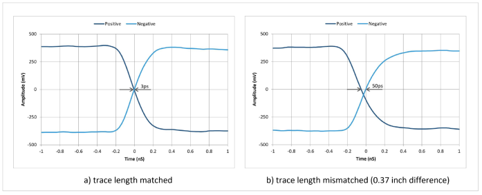
Figure 9: Intra-pair skew vs trace length matching, SiT9365 – 156.25 MHz, LVPECL driver, 3.3
5.2.2 Termination placement
Termination placement is also important. To avoid waveform degradation, place termination resistors as close as possible to receivers (load). Improperly terminated outputs cause significant signal distortion, as shown in the figure below.
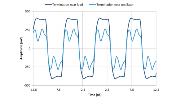
Figure 10: Waveforms measured at load for different termination placement, SiT9121 – 156.25 MHz, LVDS driver
5.3 Transmission line impedance calculation
This chapter covers the microstrip line as it is the most commonly used in layout design.
The following two figures show the impedance calculation for single-ended and differential microstrip lines.
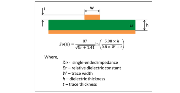
Figure 11: Single-ended microstrip line
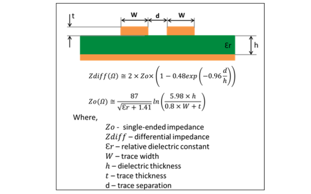
Figure 12: Differntial micro strip line
5.4 1508 CSP and 2012 QFN package layout
Sample PCB layouts for devices in 1508 and 2012 packages are shown in the following figures. It is strongly recommended that the PCB designer observe the following layout guidelines:
- Do not connect any of the pads directly to a copper polygon or a wide PCB trace. This may cause bad solder joints due to non-uniform heating transfer during the assembly process.
- Provide short length (1 to 3 mm) and thin width (~0.15 mm) traces to each pad and then to the respective copper polygon or wide trace.
- Keep mirror symmetry of the traces X-Y planes. This will prevent the rotation effect during reflow.
- Keep high-current and high-speed traces away from the CSP package:
- Route high edge-rate and noisy signals at least 1 mm away from clock-out and pin1 signal traces.
- The use of orthogonal routes is recommended to avoid signal coupling.
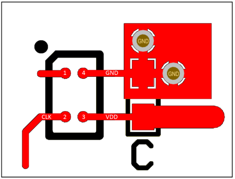
Figure 13: Layout example for 1508 CSP devices
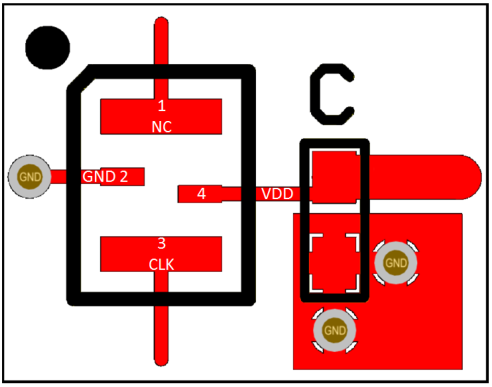
Figure 14: Layout example for 2012 (QFN) devices
5.4.1 Solder printing stencil recommendations for 1508 CSP
SiTime 1508 CSP (chip-scale packages) are constructed with a MEMS die mounted to the underside of the larger CMOS die. To ensure the necessary clearance between the MEMS die and the PCB, it is recommended to observe the following guidelines:
- Stencil thickness: 76.2 μm, laser-cut, and electro-polished
- Stencil aperture layout recommendations:
- Apertures centered on 250 μm NSMD PCB solder pads
- Two approved aperture shapes to meet customer layout design rules
- Option 1: 200 μm circle
- Option 2: 190 μm square with 25 μm radius corners
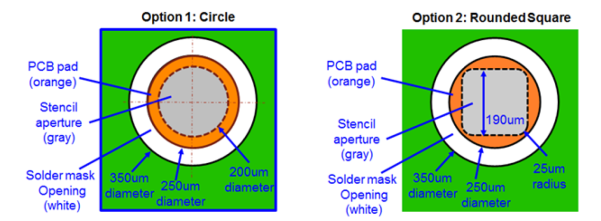
Figure 15: Solder pad stencil layout detail
5.5 SiTime specific package layout example
5.5.1 SiTime 5032 ceramic package layout
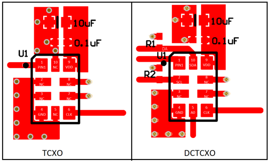
- A 0.1 μF capacitor in parallel with a 10 μF capacitor are required between VDD and GND. It is recommended to place the 0.1 μF capacitor close to the device and place the 10 μF capacitor less than 2 inches away.
- All NC pins can be soldered down with multiple vias under the GND pin for better heater dissipation.
- In OE mode for noisy environments, a pull-up resistor R1 of 10 kΩ or less is recommended.
5.5.2 SiTime OCXO 7 x 9 mm package layout
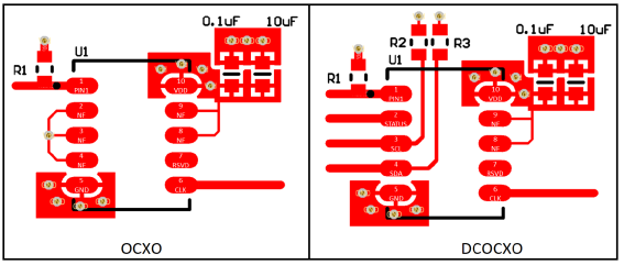
Figure 16: SiTime OCXO 7x9 package layout
- A 0.1 μF capacitor in parallel with a 10 μF capacitor are required between VDD and GND. It is recommended to place the 0.1 μF capacitor close to the device and place the 10 μF capacitor less than 2 inches away.
- All non-functional (NF) pins are recommended to connect to VDD with narrow traces (e.g., 4 to 6 μm) to avoid significant heat dissipation through these pads.
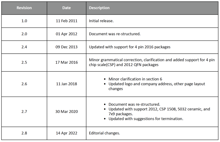
6. Revision History
Table 4: Revision History