Enhancing FPGA-based Systems with Programmable Oscillators
Jehangir Parvereshi
Sassan Tabatabaei
SiTime Corporation
990 Almanor Ave., Sunnyvale, CA 94085
Abstract
Today's FPGAs are complex systems containing many functional blocks, and multiple clocks are often used to drive different blocks. System designers have to decide how to combine external oscillators and internal resources for optimal clock-tree design. This paper will discuss the options available today to meet clock speed and jitter requirements, with a focus on programmable clock oscillators as timing references for FPGA-based systems. Topics include flexibility resulting from high-resolution frequency selection, EMI reduction techniques, and FPGA-based jitter cleaners.
1. Introduction
Complex FPGAs contain large arrays of functional blocks, or cells, that need to communicate with each other to carry out a wide range of complex operations. In addition to basic logic arrays, FPGAs include internal memory (RAM), DSP blocks, processors, phase-locked loops (PLLs) and delaylocked loops (DLLs) for timing generation, standard I/O, high-speed digital transceivers, and parallel interfaces (PCI, DDR, etc.).
Many designs use multiple clocks to drive the different blocks, and each may require a different frequency. These clocks are typically generated using a combination of external oscillators and internal PLLs and DLLs, depending on clock speed and jitter requirements. Clock speeds for some functions are determined by application, whereas the designer may select frequency for other parts of the system.
2. Multiple Clock Frequencies
Clocks associated with I/O interfaces need to run at industry-standard frequencies in order to ensure interoperability between different systems. Examples include 100 MHz for PCI Express, 75 MHz for SATA or 33.333 MHz for PCI.
Users can usually select the frequency for clocks that drive processors or state-machine engines. This flexibility allows designers to choose a frequency that optimizes speed, power or resource usage.
When optimizing for speed, it may seem straightforward to use the highest frequency possible to maximize the number of operations per second. The clock period jitter, however, must be low enough so that the minimum clock period is greater than the critical timing path in the design.
Internal PLLs in an FPGA can be used to synthesize a higher frequency clock from a lower frequency external reference oscillator. This can be an effective method for frequency selection if the PLL has high frequency resolution and low jitter. Low noise, fractional-N PLLs can meet most specifications when driven by a simple external oscillator.
Many FPGAs, however, use integer PLLs with a ring voltage-controlled oscillator (VCO) because they are easy to design and consume very little power. The problem with this type of PLL is the trade-off between frequency resolution and jitter.
A typical integer PLL includes a pre-divider (P), feedback divider (M), and post-divider (N), as shown in Figure 1 . The output frequency is defined by equation 1.
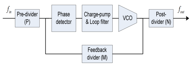
Figure 1. Block diagram of a typical integer PLL
While the output jitter depends on phase noise of both the reference clock and the internal VCO, the contribution of the internal VCO usually dominates. The higher the bandwidth of the PLL, the lower the VCO phase noise and the lower the overall jitter. The maximum PLL bandwidth is defined as a function of the pre-divide ratio as follows:
A more conservative value for the bandwidth, commonly used when specifying actual PLLs, is given by equation 3:
Increasing the bandwidth to improve jitter is usually desirable. One problem is that large values of P are typically required to achieve high enough frequency resolution, limiting the maximum PLL bandwidth.
3. Optimizing PLL Design
One approach that allows both high frequency resolution and low jitter is to use a programmable oscillator as an external reference. This puts lower demands on the internal PLL while providing required performance. Programmable external oscillators can use a higher frequency reference, which can reduce required pre-divide ratios, allowing higher PLL bandwidth.
As an example, consider an application requiring a 56 MHz clock with 10 ps RMS jitter. Figure 2 shows two designs, one using a standard 25 MHz reference and the other using a non-standard 28 MHz reference from a programmable oscillator.
Design a requires a large value of P, resulting in a bandwidth of 50 kHz (as calculated by equation 3) and jitter of 30 ps, which is out of specification. Design b takes advantage of frequency programmability to select an input frequency that allows for the pre-divide ratio to be unity, resulting in a PLL bandwidth of 1.4 MHz. Jitter is less than 10 ps rms, meeting the stated requirements.
Programmable oscillators can include either quartz or silicon MEMS resonators, but MEMS-based oscillators have the advantage of being readily available in a variety of industry-standard plastic packages and any desired input frequency. They provide a costeffective solution to meet the jitter requirements of demanding FPGA applications.
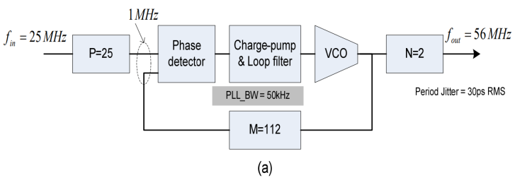
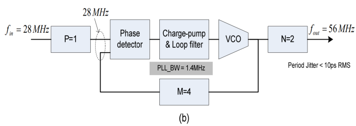
Figure 2. Two PLL designs: (a) standard frequency reference clock and (b) flexible frequency reference clock, allowing higher PLL bandwidth and lower jitter
4. EMI Reduction
One potential concern about oscillators is generation of unwanted electromagnetic interference (EMI). Programmable oscillators can incorporate features that are effective at reducing EMI emitted by the oscillator. Two options that can be useful for FPGA devices are edge rate tuning and spread-spectrum clocking (SSC) [2].
Edge rate tuning, or increasing the rise and fall time of the clock signal, reduces the EMI generated by higher order clock harmonics radiated from the clock traces in a specific circuit. The peak clock signal remains constant, avoiding the voltage swing reduction experienced when using filters to reduce EMI. Figure 3 shows the amplitude of clock harmonics as a function of rise time, demonstrating the effectiveness of edge rate tuning in reducing EMI from higher order harmonics. Fall time is assumed to be equal to rise time, providing a symmetric signal.
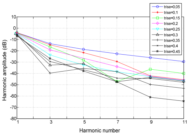
Figure 3. Clock signal harmonic amplitude as a function of rise/fall time
There are two methods for increasing the rise/fall times. The first, increasing load capacitance, has the disadvantage of also increasing current consumption. Programmable oscillators enable the option of adjusting the output current drive instead, a method that does not affect current consumption. This approach is preferred.
While edge rate tuning can be effective, it only works on one circuit at a time and only on clock harmonics radiated from the clock traces. Moreover, for systems with high-speed clocks it may not be possible to adjust the rise/fall time sufficiently to achieve the desired EMI reduction.
SSC is an EMI reduction technique that reduces peak electromagnetic radiation emitted from the clock tree and data lines clocked with the tree by spreading out the energy of the clock signal over a larger frequency range. This reduces the peak power at a given frequency and is effective for both the primary carrier frequency and higher harmonics. The higher the clock frequency, the greater is the EMI reduction. This makes SSC very desirable for high frequency applications.
Frequency spread options include center spread, centered around the carrier frequency, or downspread, where the modulation is concentrated below the nominal frequency. Figure 4 demonstrates the SSC modulation example with 2% down-spread.
SSC is an especially attractive option for FPGAs, because it reduces EMI from all functional blocks that share the same clock source. Other approaches to reducing EMI, such as trace filtering and rise/fall time control, tend to decrease EMI in only a certain section of the system.
Figure 4. SSC modulation to reduce EMI
5. In-system Frequency Programming
Programmable oscillators can use digital control to program frequency in the system dynamically. One application for such devices is jitter cleanup in networking, telecom, video/audio, and instrumentation applications. Such digitally controllable oscillators (DCXOs) achieve superior frequency control by directly driving the digital input of the PLL feedback divider or fractional-N PLL modulator. [1]
DCXOs driven by FPGAs enable dynamic control of loop bandwidth. For example, bandwidth can be set higher to reduce locking time and improve the tracking dynamics, or set lower for better jitter cleanup performance.
Several parameters are important when designing DCXOs: frequency resolution, update rate and update delay. DCXO quantization noise is related to frequency resolution and update rate, and should be well below the native phase noise of the oscillator. As the example in figure 5 shows, at an update rate of 25,000 updates/s, resolution of 1 ppb results in sufficient low phase noise from the DCXO.
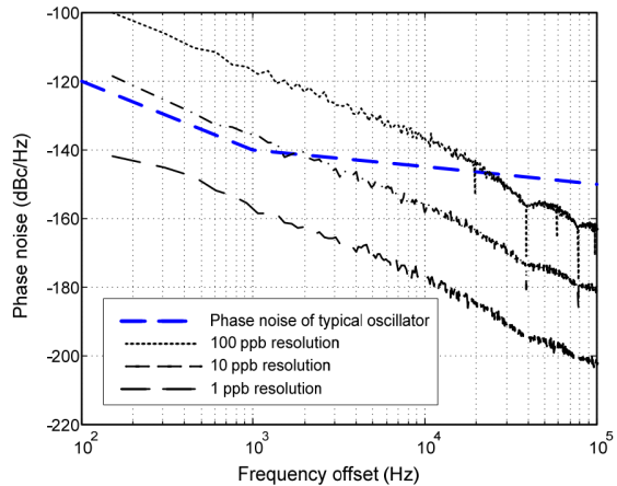
Figure 5. Quantization-induced phase noise at update rate
of 25 kHz for DCXOs with different frequency resolution
It is important to consider the contribution of update rate to the final phase noise. Typically, low update rates causes any the error signals from the phase detector and loop filter to be integrated by the DCXO over a longer time, which results in higher phase noise. For a DCXO with 1 ppb resolution, update rates as low as 2500 updates/s can be tolerated without adverse effect on phase noise, as seen by the data in figure 6. High precision DCXOs available today can provide 1 ppb or better resolution, which effectively eliminates any quantization impact on output phase noise even at relatively low update rates.
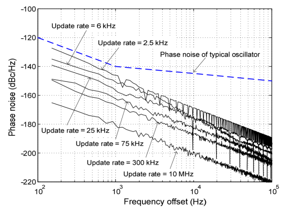
Figure 6. The effect of update rate on phase noise for a DXCO with 1 ppb frequency resolution
The update rate and delay of the DCXO contribute to the overall stability of the loop filter. When both the update rate and inverse of the update delay are at least 10 times higher that the target loop bandwidth, the loop will be stable. This means that for a 1 kHz loop bandwidth, the update rate should be higher than 10 kHz and the update delay shorter than 100 µs. DCXOs with these specifications are readily available.
6. Jitter Cleaner
Jitter clean-up techniques are often needed when locking to a noisy system clock, in order to generate a stable clock signal with low phase noise and low jitter. An important component of synchronization or jitter clean-up PLLs are high precision oscillators with either analog (VCXO) or digital (DCXO) frequency control.
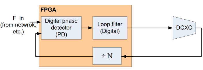
Figure 7: Block Diagram of a implementation of a FPGA and DCXO based jitter cleaner solution
Today's high performance DCXOs can be designed to sufficiently reduce quantization noise, enabling them to be a solution for low bandwidth PLLs. Jitter cleanup has been successfully implemented using only an FPGA and a DCXO chip as shown in Figure 7, demonstrating such concept.
7. Summary
Programmable oscillators with fractional-N PLLs function well as external reference clocks for FPGAs. The advantage of programmable input frequency makes it possible to design PLLs with very low jitter. Programmability makes it easy to add features such as edge rate control and SSC for EMI reduction or digital control for improved stability to optimize system performance. Using FPGAs with state-ofthe-art programmable DCXOs offers the added advantage of being a very cost effective and highly parameterizable jitter-cleaning solution for noisy clock references.
8. References
[1] Sassan Tabatabaei, “Analysis of High-Stability Controlled Oscillators for Low-Bandwidth PLLs” – DESIGN East, September 2012.
[2] Sassan Tabatabaei, “Clocking Strategies for EMI Reduction”, Interference Technology – EMC Test and Design Guide, November 2010.