I2C/SPI Programmable Oscillators
Contents
1. Introduction
2. Theory of Operation
2.1 Any Frequency Function
2.2 Digital Control
2.3 Additional Functions
3. Any Frequency Programming Algorithm
3.1 Post-Divider and Feedback Divider Selection
3.2 Writing Post-Divider and Feedback Divider to the Device
4. Frequency Pulling
5. Additional Functions
5.1 Output Enable
5.2 Driver Control
6. Application
6.1 SDI
6.2 Ethernet
6.3 SONET/SDH
7. Evaluation Tools
Appendix A: I2C/SPI oscillators Calculation Example
SiT3521 - 1 to 340 MHz I2C/SPI Oscillator
SiT3522 - 340.000001 to 725 MHz I2C/SPI Oscillator
Appendix B: Frequency Pulling Examples
Example 1
Example 2
1. Introduction
SiTime Elite Platform™ I2C/SPI oscillators (SiT3521/2) are user-programmable devices that enable the user to reprogram the clock and set the device output frequency to any supported value during operation using a digital interface (I2CI or SPI). Two modes of operation are supported: 1) any-frequency mode with the capability to set the frequency to a new value within a wide frequency range (output is disabled for a short time) and 2), digitally controlled oscillator (DCO) mode that allows the output frequency to be continuously pulled within the specified pull range. Pull range can be changed in-system to one of 16 available pull range options. Additionally, I2C/SPI oscillators allow users to control the output enable (OE) state of the device and output driver settings (e.g. output swing). The SiT3521 (1 to 340 MHz) and the SiT3522 (340.000001 to 725 MHz) I2C/SPI oscillators support three signaling types: LVPECL, LVDS, and HCSL.
I2C/SPI oscillators, with digital control, offer multiple advantages compared to VCXOs:
- Frequency control resolution as low as 5E-12 – This high resolution minimizes accumulated time error in synchronization applications.
- Lower system cost – Traditional VCXOs require a digital to analog converter (DAC) to drive the control voltage input. In an I2C/SPI oscillator, the frequency control is achieved digitally by writing to the control registers using a serial interface, eliminating the need for a DAC.
- Better noise immunity – The analog signal that is used to drive the voltage pin of a VCXO can be sensitive to noise and the trace over which the signal is routed can be susceptible to noise coupling from the system. Because I2C/SPI devices are digitally controlled oscillators (DCOs) and frequency control is performed over a digital interface, they do not suffer from analog noise coupling.
- No frequency pull non-linearity – The frequency pulling is achieved via a fractional feedback divider of the PLL, eliminating any pull non-linearity that is sometimes associated with quartzbased VCXOs. Better pull range linearity improves dynamic performance in closed loop operations.
- Programmable wide pull range – Because the pulling mechanism is achieved via a fractional feedback divider, it is not constrained by resonator pullability as it is in quartz-based solutions. SiTime I2C/SPI oscillators have 16 frequency pull range options from ±6.25 ppm to ±3200 ppm, offering system designers great flexibility.
2. Theory of Operation
Figure 1 shows a high-level block diagram of the I 2 C/SPI oscillator.
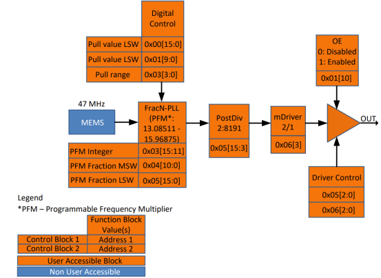
Figure 1. DE I 2 C/SPI Oscillator High-Level Block Diagram
2.1 Any Frequency Function
After power-up, a user can reprogram the device to any frequency within the supported range. To program the device to the target output frequency, the user should calculate the post-divider, feedback divider, and mDriver values and write them to the device. For output frequencies above 340 MHz (SiT3522 family), the mDriver value should be calculated and written to the device along with the post and feedback dividers. The only one input for this calculation is target output frequency value. The feedback divider value should be written first and post-divider value last. After the first word is written to the device (which would be the feedback divider’s most significant word), its output is disabled. After the post-divider value is written, the engine inside the chip applies the new settings, tracks the PLL lock signal, and enables the output driver after the PLL is locked (see Figures 2 and 3).
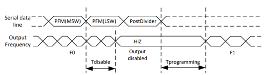
Figure 2. Frequency Reprogramming Timing Diagram (SiT3521)
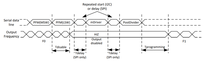
Figure 3. Frequency Reprogramming Timing Diagram (SiT3522)
2.2 Digital Control
The device powers up at the nominal operating frequency and pull range specified by the ordering code. After power-up, both the pull range and output frequency can be controlled via digital interface writes to the respective control registers. The maximum output frequency change is constrained by the pull range limits. Pull ranges are specified in the form of half of the peak-to-peak deviation (e.g. ±100 ppm which is 200 ppm peak-to-peak).
The pull range is specified by the value loaded to the digital pull range control register (Reg2[3:0]). The 16 pull range choices are documented in the control register and range from ±6.25 ppm to ±3200 ppm. Table 1 below shows the frequency resolution vs. pull range programmed value along with the corresponding programming codes.

Table 1: Frequency Resolution vs. Pull Range
The frequency offset (in ppm) is specified by the 26 bit DCO frequency control register in 2’s complement format. The power-up default value is 00000000000000000000000000b which sets the output frequency at its nominal value (0 ppm). To change the output frequency, a frequency control word is written to Reg0[15:0] (least significant word, LSW) and Reg1[9:0] (most significant word, MSW). The LSW value should be written first followed by the MSW value; the frequency change is initiated after the MSW value is written. After the MSW pull value is written, control logic changes the feedback divider value (during Tdelay timeframe) to accommodate the new frequency. Then the output frequency starts changing and settles to 1% of the final frequency value within the Tsettle timeframe (see Figure 4).
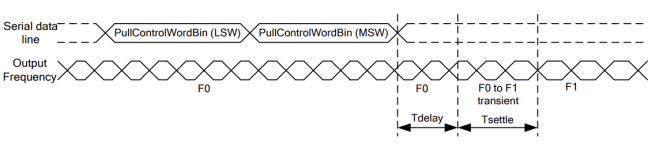
Figure 4. Frequency Pulling Timing Diagram
The device output is not disabled during frequency change. Therefore if the software output enable (OE) control function is enabled, a user can disable output manually for frequency change period.
Important note: maximum digital control update rate is 38 kHz regardless of digital interface bus speed.
2.3 Additional Functions
Output is enabled/disabled within the Tenable/Tdisable time after the control word is written to the device.
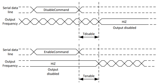
Figure 5. Output Enable/Disable Timing Diagram
All other settings (e.g. driver control) are applied immediately after the write transaction.
3. Any Frequency Programming Algorithm
The only input from the user for the dividers calculation is target output frequency value. Other inputs are dividers allowed ranges.
3.1 Post-Divider and Feedback Divider Selection
Generally there are three steps for dividers calculation. Therefore for SiT3521 devices, only the first step implementation is required:
- Step 1: PostDiv and PFM calculation for mDriver = 2.
Find the lowest allowed post-divider value which gives the programmable frequency multiplier (PFM ) value (see equation 3) within the allowed PFM range of 13.08511 to 15.96875 (see equation 2):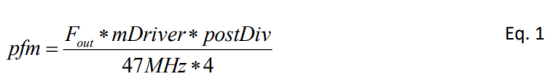 where:
Fout – target output frequency (1 to 340 MHz for SiT3521; 340.000001 to 725 MHz for SiT3522);
postDiv – post divider value within 2:8191 range;
mDriver = 2.
For the 1 to 340 MHz SiT3521 family, the selected combination will be the final one. Steps 2 and 3 should be omitted. - Step 2: PostDiv and PFM calculation for mDriver = 1.
Step 2 is similar to step one with two changes: mDriver = 1 and allowed postDiv values are 3, 5, and 7. This step does not apply for SiT3521. 3. - Step 3: Select final dividers combination.
The criterion for the final dividers combination selection from calculated in steps 1 and 2 is the lowest PFM value. If one of the steps does not have a valid combination, the one from the other step is selected as final. If there are no valid combinations for both steps, the frequency is out of the supported range. This step does not apply for SiT3521. - Write selected combination of PFM (pfm), post-divider (postDiv) and mDriver values to the device.
3.2 Writing Post-Divider and Feedback Divider to the Device
The selected combination of post-divider, feedback divider, and mDriver values should be converted to binary words and then written to the device’s control registers. Number conversion, conditioning, and write procedure are as follows:
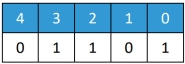
1. Convert feedback divider value to binary word:
a) 32 bits are intended for feedback divider value: 5 bits for integer and 27 for fractional parts:
I. Round the feedback divider value (pfm) towards zero to get the integer decimal part (pfmInt)
II. Subtract the integer decimal part (pfmInt) from the feedback divider value (pfm) to get the fractional decimal part (pfmFrac)
III. Convert the integer decimal part (pfmInt) to a 5-bit binary word (pfmIntBin). Since the feedback divider is always positive, no sign bit should be used
IV. Multiply the fractional decimal (from step 1.a.ii) by 227, round to the nearest integer and convert the result to a 27-bit binary word (pfmFracBinFinal). Since the fractional part of the feedback divider is always positive, no sign bit should be used.
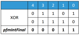
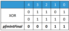
b) Execute bitwise XOR operation on feedback divider integer part and 01110b mask (pfmIntFinal)
2. Convert the post-divider value to a binary word:
a) 13 bits are intended for the post-divider value
b) Convert the post-divider value (postDiv) to a 13-bit binary word (postDivBin). Since post-divider is always positive, no sign bit should be used
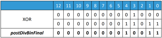
c) Execute the bitwise XOR operation on the post-divider binary word and 0000000011011b mask to get the final post divider word (postDivBinFinal)
3. Convert mDriver to a binary value
a) One bit is intended for mDriver control where: 0b sets mDriver = 2 and 1b sets mDriver = 1 (bypass)
4. Read back Reg5 (address 0x05) and Reg6 (0x06, can be omitted for SiT3521) registers values from the device and mask bits 2:0 which should not be changed
5. Form register content for writing:
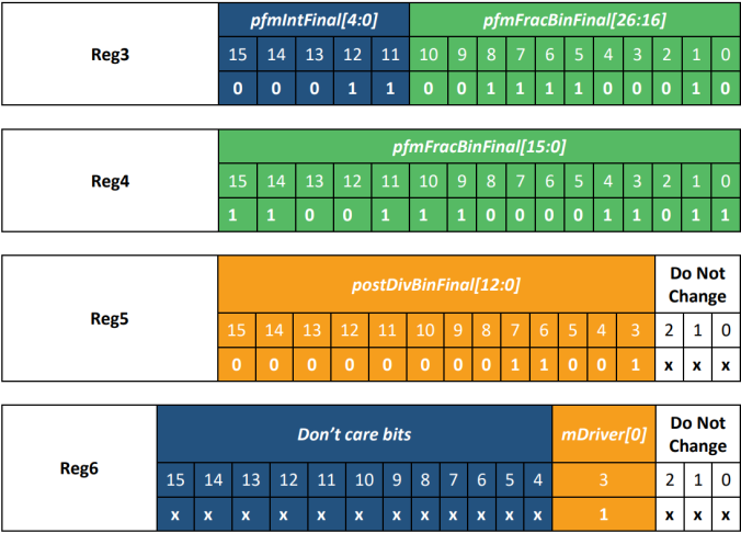
a) Reg3 (address 0x03):
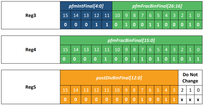
I.Reg3[15:11] = pfmIntFinal[4:0]
II. Reg3[10:0] = pfmFracBinFinal[26:16]
b) Reg4 (address 0x04):
I. Reg4[15:0] = pfmFracBinFinal[15:0
c) Reg5 (address 0x05):
I. Reg5[15:3] = postDivBinFinal[12:0]
II. Reg5[2:0] = Do not change
d) Reg6 (address 0x06):
I. Reg6[3] = mDriver[0]
II. Reg6[2:0] = Do not change
6. Write registers to the device in the following sequence:
a) SiT3521
I. Reg3
II. Reg4
III. Reg5
b) SiT3522
I. Reg3
II. Reg4
III. Reg6
IV. Reg5
4. Frequency Pulling
Following are the procedures for frequency pulling of SiTime I2C/SPI oscillators:
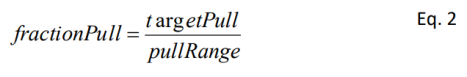
1. Calculate the fraction of the target pull value (targetPull) relative to the pull range (pullRange):
2. Multiply the fraction of the target pull value by the full half scale word value and round to the nearest whole number:
3. Convert the result of step 2 to two’s complement binary (pullControlWordBin)
4. Read Reg1 value from the device as it includes control bits for other settings
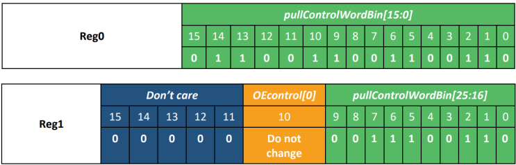
5. Form the register content for writing:
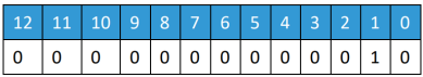
a. Reg0[16:0] – pullControlWordBin[15:0] (LSW)
b. Reg1[9:0] – pullControlWordBin[25:16] (MSW)
c. Reg1[15:10] – Do not change
6. Write registers with the sequence as follows:
a. Reg0
b. Reg1
5. Additional Functions
5.1 Output Enable
The output driver can be enabled or disabled through control registers. (The corresponding part number option should be selected to enable this function. Refer to the datasheet of selected product familiy). To enable the output driver, Reg1[10] (address 0x01) should be set to 1; to disable set to 0.
Important note: By default (at startup) output is disabled in this mode and should be enabled by appropriate write operation after start-up.
5.2 Driver Control
Output swing can be controlled through a digital interface to compensate for the signal amplitude drop in the transmission line across the supported frequency range. For this purpose, reg5[2:0] and reg6[2:0] are used. Table 2 below shows register values based on the output driver and frequency which should be written to the device to accommodate output swing specification.
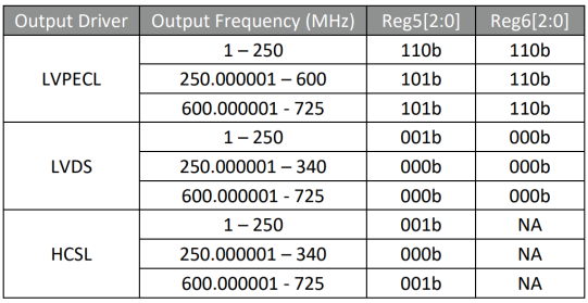
Table 2: Driver settings
6. Application
Some applications use multiple oscillators (XOs) with different output frequencies and switch between them for each particular frequency needed (see Figure 6). The SiT3521/2 I2C/SPI oscillators, based on SiTime’s Elite PlatformTM with in-system programmability added, are designed to replace this complicated and costly block. The use of multiple oscillators, plus a clock switch, consumes a large area on the board and increases BOM cost. Using a single oscillator that can be re-programmed to any frequency reduces the PCB area, reduces the BOM cost, and simplifies the design. Following are a few application examples that are ideal for I2C/SPI in-system programmable oscillators.
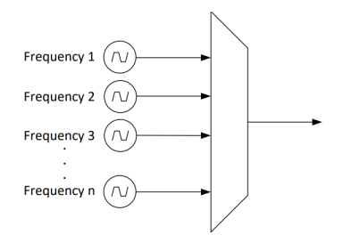
Figure 6. Example Multi-Frequency Clocking Architecture
6.1 SDI
Digital video transmission rates have increased to support high-definition video. 3G-SDI/6G-SDI/12G-SDI standards were developed by SMPTE (Society of Motion Picture and Television Engineers) to define the requirements for high-performance video systems. In particular, these standards define the requirements for clocks used in these systems which must meet ever tighter jitter specifications as video data rates increase. Timing solutions must also accommodate multiple frequencies required by legacy video standards for backward compatibility.
Typical reference clock frequencies required by different video standards include 74.25 MHz and 74.25/1.001 MHz, 148.5 MHz and 148.5/1.001 MHz, 297 MHz and 297/1.001 MHz. In order to support multiple video standards, the clocking solution must provide this entire list of standard frequencies.
Some clocking architectures, such as those used in SDI applications, traditionally use multiple discrete XOs with a clock multiplexer to select different frequencies. Using a single-chip clocking solution, such as SiTime I2C/SPI oscillators, provides an optimized solution for supporting multiple reference frequencies by simply reprogramming the device using a serial interface. Additionally, the low jitter performance of these devices easily meets the requirements defined by SDI standards.
SDI re-clocker applications also require a voltage control function for the clock. The digital control function of SiTime I2C/SPI oscillators can be used instead. This solution eliminates the need to have a DAC in the system, eliminates VCXO non-linearity issues, and is much more immune to noise.
6.2 Ethernet
Ethernet is a family of computer networking technologies commonly used in local area networks (LAN), metropolitan area networks (MAN), and wide area networks (WAN). Similarly to SDI applications, Ethernet applications have multiple standards developed by the time including 1 GbE, 2.5GBASE-T, 5GBASE-T, 10 GbE, 40 GbE, and 100 GbE. Equipment that supports multiple standards might use different reference frequencies optimized to provide needed data rate such as 125 MHz, 156.25 MHz, 161.1328 MHz, 312.5 MHz, and 322.265625 MHz. SiTime I2C/SPI oscillators provide a flexible clock solution to support all of these frequencies in a single-chip. Additionally, excellent jitter performance makes SiTime I2C/SPI oscillators an ideal solution for Ethernet applications.
6.3 SONET/SDH
Synchronous optical transport networks based on SONET/SDH and OTN technology are well suited to meet the requirements of telecom transmission systems, and are now commonplace in such applications. Network specifications, such as the ITU-T G-series or Telcordia GR-series, describe the jitter performance of networks and network equipment and set limits on the amount of jitter that devices may generate, tolerate, and transfer. Multiple SONET/SDH interfaces provide different data rates and need different reference frequencies in the systems supporting multiple interfaces such as 77.76 MHz, 155.52 MHz, and 622.08 MHz. SiTime I2C/SPI oscillators provide an ideal timing solution for SONET/SDH applications because they meet jitter requirements and deliver any frequency for the system.
7. Evaluation Tools
The SiT6712EB evaluation board (EVB) is designed for use with SiTime I2C/SPI oscillators that support the differential signaling outputs in the 5.0 x 3.2 mm 10-pin QFN package. This EVB enables users to evaluate all aspects of the I2C/SPI programmable oscillators including signal integrity, phase noise, phase jitter, and reprogramming of the output frequency via I2C/SPI interfaces.
EVB Features:
- Support for SiT3521 (1 to 340 MHz) and SiT3522 (340 to 725 MHz) I 2 C/SPI programmable oscillators
- Probing points for output frequency measurements
- Support for LVPECL, LVDS, and HCSL output signal types
- Support for waveform measurements
- Support for phase noise and phase jitter measurements
- Connector access to I2C and/or SPI interfaces
- Connector access for current consumption measurements
SiTime typically ships the EVB pre-configured with the I2C/SPI programmable oscillator device specified by the user.
More details can be found in SiT6712EB user manual.
Appendix A: I2C/SPI oscillators Calculation Example
SiT3521 – 1 to 340 MHz I2C/SPI Oscillator
This section shows examples of the post-divider and feedback divider calculation and conversion to the binary words. 156.25 MHz is the target output frequency in this example.
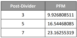
1. The lowest post-divider giving PFM within allowed range is highlighted in green:
2. Converting calculated feedback divider value to binary word:
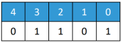
a. Round pfm to zero to get pfmInt:
pfmInt = 13
b. Get the fractional part of feedback divider value:
pfmFrac = pfm – pfmInt = 0.29787
c. Five bits are dedicated to the integer part of the feedback divider and converted decimal value to binary word is:
d. To get the final integer feedback divider binary word, the value obtained in step 5d is masked as follows:
e. Fractional part has 27 bits dedicated for it. Before the conversion to binary word, multiply by 227 :
0.29787 * 227 = 39979434.63936 ≈ 39979435
The multiplied value converted to binary word is (pfmFracBinFinal):

3. Converting post-divider value to binary word:
a. 13 bits are dedicated for the post-divider and decimal value converted to binary word is:
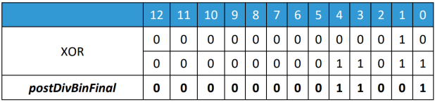
b. To get the final binary word, the value obtained in step 6a is masked as follows:
4. Binary values of feedback divider and post-divider are mapped to the dedicated registers as follows:
SiT3522 – 340.000001 to 725 MHz I2C/SPI Oscillator
This section shows examples of the post-divider and feedback divider calculation and conversion to the binary words. 622.08 MHz is the target output frequency in this example.
- Step 1: PostDiv and PFM calculation for mDriver = 2. The lowest post-divider giving PFM within the allowed range is highlighted in green:
- Step 2: PostDiv and PFM calculation for mDriver = 1. This step does not give any valid combination:
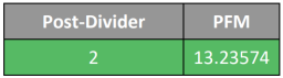
- Step 3: Select final dividers combination. As step 2 does not have a valid combination, the value from step 1 is selected: postDiv = 2; pfm = 13.23574; mDriver = 2.
- Converting calculated feedback divider value to binary word:
a. Round pfm towards zero to get pfmInt:
pfmInt = 13
b. Get fractional part of feedback divider value:
pfmFrac = pfm – pfmInt = 0. 23574
c. Five bits are dedicated to the integer part of the feedback divider and converted decimal value to binary word is:
d. To get the final integer feedback divider binary word, the value obtained in step 5d is masked as follows:
e. Fractional part has 27 bits dedicated for it. Before the conversion to binary word it gets multiplied by 227:
0. 23574 * 227 = 31,641,115.451915 = 31,641,115
The multiplied value converted to binary word is (pfmFracBinFinal):

5. Converting post-divider value to binary word:
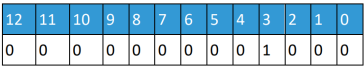
f. 13 bits are dedicated for the post-divider and decimal value converted to binary word is:
g. To get the final binary word, the value obtained in step 6a is masked as follows:
6. Converting mDriver to binary value: 0x06[3] = 0 as mDriver is 2.
7. Binary values of feedback divider and post-divider are mapped to the dedicated registers as follows:
Appendix B: Frquency Pulling Examples
Pull range: ±200 ppm (pullRange)
Default output frequency: 156.25 MHz
Desired output frequency: 156.2640625 MHz (targetPull = +90 ppm)
Following the frequency pulling procedure:
- fractionPull = +90 / 200 = 0.45
- pullControlWordDec = round(0.45 * 225 -1) = round(15,099,493.95) = 15,099,494
- pullControlWordBin = 111001100110011001100110b = 0xE66666

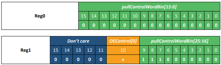
4. Register content for the writing is:
Pull range: ±200 ppm (pullRange)
Default output frequency: 122.88 MHz Desired output frequency: 122.873856 MHz (targetPull = -50 ppm)
Following the frequency pulling procedure:
- fractionPull = -50 / 200 = -0.25
- pullControlWordDec = round(-0.25 * 225 -1) = round(-8,388,607.75) = -8,388,608
- pullControlWordBin = 11100000000000000000000000b = 0x3800000 25 24 23 22 21 20 19 18 17 16 15 14 13 12 11 10 9 8 7

4. Register content for the writing is: