Driving Multiple Loads with 32 kHz Nano-Power MEMS Oscillators
Optimizing board space and managing power consumption of wearable devices is critical in sustaining competitiveness within this fast-growing consumer segment. With less power consumed, battery life is extended or provides the option to reduce the battery size. MEMS-based reference clocks offer an alternative to traditional quartz crystal timekeeping components, with advantages including a significant footprint reduction, improved accuracy, and lower system power. In addition, the capability to drive multiple loads with one ultra-small, nano-power oscillator is one way in which MEMS are supporting these improvements.
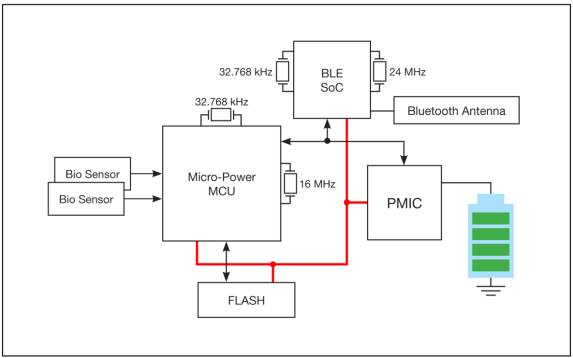
Figure 1: Block diagram of wearable showing key components
A wearable device typically comprises a low-power MCU and a low-power RF transceiver BLE (Bluetooth Low Energy is ubiquitous in today’s wearable devices) and sensors as shown in the block diagram of Figure 1. The MCU and BLE devices consume a high percentage of the system power budget and are designed to spend most of the time in sleep mode to conserve power. In this mode all high-frequency oscillators and PLLs are disabled. The only continually operating clock sources are those derived from the always-ON 32 kHz resonator-driven oscillators:
- 32 kHz oscillator used by the MCU RTC and watch-dog timer
- 32 kHz oscillator as the BLE sleep clock reference
An alternative solution which offers both space and power savings is to use one MEMS-based 32 kHz SiT1532/1552 or SiT1630 ultra-small, nano-power oscillator and TCXO to replace multiple 32 kHz quartz crystal-based oscillators. The output driver of one SiT15xx/16xx can easily drive the 32 kHz crystal inputs of MCU and BLE devices without any signal reflections.
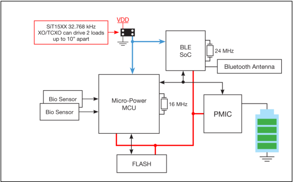
Figure 2: Typical connection of SiT15xx oscillator to multiple ICs
Figure 2 shows how one SiT15xx oscillator can be used to replace two 32 kHz crystal resonators. The SiT15xx has typical rise/fall times of 20 ns when driving a 5 pF load. The SiT15xx output driver is capable of driving a combined trace and IC load of up to 100 pF without reflections, eliminating signal integrity issues.
Signal integrity can be demonstrated through IBIS simulations as shown in the following graphs with various transmission line conditions and output drive settings. The simulation setup is shown in Figure 3. IBIS models of a SiT1532 LVCMOS and D26 Nano-Drive™ output drivers with Vdd = 1.8V were used. To emulate the load seen by the SiT15xx a capacitor of various pF values is placed at the end of each transmission line.
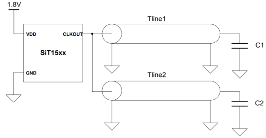
Figure 3: IBIS simulation setup
Figure 4 and Figure 5 show clock signal waveform at each load (C1, C2) obtained during IBIS simulations with the following setup:
- SiT1532 output driver = LVCMOS
- 50Ω transmission line length = 6 inches
- C1 = 20 pF; C2 = 30 pF
The capacitance of each trace is ~17 pF and the total load seen by the SiT1532 output driver is 17pF*2+20pF+30pF = 84pF. As seen from the waveforms, the capacitive loads increase rise/fall time but does not degrade the clock waveform at either load.
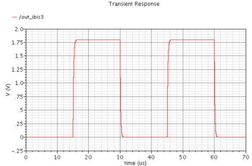
Figure 4: SiT1532-DCC waveform across C1 (20pF) at the end of a 6-inch 50 Ω transmission line
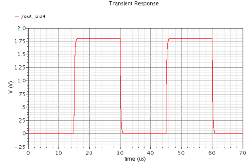
Figure 5: SiT1532-DCC waveform across C2 (30pF) at the end of a 6-inch 50 Ω transmission line
Figure 6 shows the waveform of a LVCMOS drive SiT532 at C1 at the end of a 100Ω 10-inch trace; C1 = C2 = 5 pF.
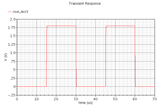
Figure 6: SiT1532-DCC waveform across C1 (5pF) at the end of a 10-inch 100 Ω transmission line
Figure 7 shows the waveform of SiT1532 with a D26 NanoDrive output drive at C1 at the end of a 100Ω 10-inch trace; C1 = C2 = 5 pF.
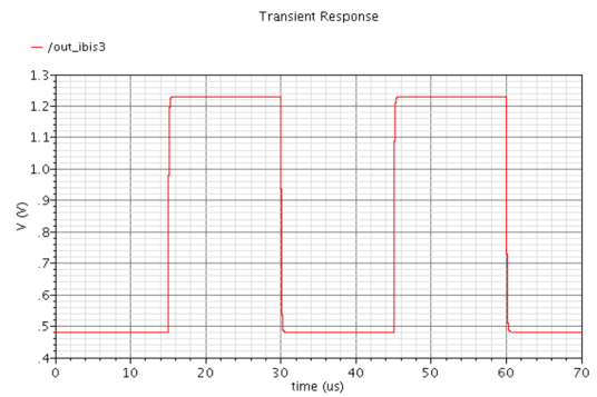
Figure 7: SiT1532-D26 waveform across C1 (5pF) at the end of a 10-inch 100 Ω transmission line
In most applications, a 32 kHz SiT15xx oscillator provides an excellent clock source for several ICs within the system. This helps decrease the total power consumption of a system, increase its reliability and decrease the board size and BOM. SiTime provides IBIS models for SiT15xx oscillators and strongly recommends running simulations to validate the signal integrity of the specific PCB configuration.