Content
3.1 1-Wire Programming Interface
3.1.2 Interfacing with an FPGA
1 Introduction
High stability controlled oscillators are devices that contain circuitry that allows the frequency to be changed with high resolution. This document describes only high stability controlled oscillators with frequency control in a narrow range lower than ±1% from its nominal frequency. Oscillator frequency can be set very accurately, which is useful in synchronization, jitter cleaner, and clock recovery applications in high-performance digital communication systems. The most popular types of high-stability controlled oscillators are as follows:
1. Voltage-controlled crystal oscillators (VCXO)
2. Digitally-controlled crystal oscillators (DCXO)
Both types of controlled oscillators may be used for high-performance digital communications systems which employ a phased locked loop (PLL) that operates within a small frequency range. Such PLLs typically have very low bandwidth, e.g. less than 1 kHz, to filter out much of the phase noise and jitter from the reference input clock.
DCXO-based PLLs offer several advantages over VCXO-based designs. One benefit is reduced system cost because on-system digital-to-analog converters and other controlled analog sources are not required when designing with a DCXO. Figure 1 shows two implementations of a PLL; one based on a DCXO and the other designed with a VCXO. High stability DCXOs, which exhibit ± 1% or better linearity, are ideal for all digital low-bandwidth PLLs (ADPLL).
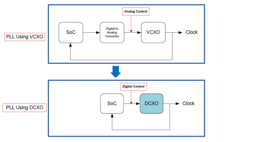
Figure 1: Simplifying PLL implementation with a DCXO.
2 DCXO vs. VCXO Performance
Analog and digitally controlled oscillators differ in performance across a few parameters: pull range, gain, linearity, and close-in phase noise. Unless noted, most of the performance parameters are applicable to both VCXO and DCXO.
Pull range (PR) is the guaranteed value of frequency deviation from nominal frequency under typical conditions, expressed in ppm. To reach higher PR in quartz-based VCXOs, generally, quartz crystals with lower Q are used. Quartz crystals with low Q are more “pullable”, but frequency stability is degraded. Thus, designers have to choose between the minimum PR required by the application while meeting the required minimum frequency stability. Typically, VCXOs exhibit a maximum PR of ±150 ppm, while DCXOs can achieve PR > ±1000 ppm with no impact to frequency stability. For instance, PR of a quartz-based DSV753SV VCXO is ±150 ppm, while PR of a MEMS-based SiT3907 DCXO is up to ±1600 ppm.
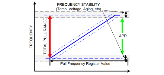
Figure 2: DCXO Frequency vs code plot showing impact of Fstab and Faging on PR
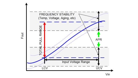
Absolute pull range (APR) is the guaranteed controllable frequency range around nominal frequency over all environmental and aging conditions, expressed in ppm. It is effectively the pull range value after taking into account frequency stability tolerances over variables such as temperature, power supply voltage, and aging.
Where; Fstability is the device frequency stability due to initial tolerance and variations across temperature, power supply, and load. Faging is the frequency deviation due to aging. All parameters in this equation are expressed in ppm.
Figures 2 and 3 illustrate the relationship of Fstability and Faging on PR for DCXO and VCXO, respectively.
VCXO gain (kv) is the ratio of frequency variation for a given input voltage variation. This ratio is expressed as Hz/V or ppm/V and average kv can be calculated as:

Where;
Fmax is maximum frequency at voltage Vmax and Fmin is maximal frequency at voltage Vmin.
This parameter is applicable to VCXOs. For instance, measured kv of the quartz-based DSV753SV VCXO is 78 ppm/V.
DCXO gain (kd)is the minimum frequency resolution step which can be achieved within a PR. Unlike VCXOs, DCXO frequency is controlled by digital code written to on-chip “pull” registers. The lower the pull range, the higher the step resolution. This is expressed in either parts-per-billion (ppb) or ppm. For example, the SiT3907 has kd as low as 1 ppb step resolution.
Linearity of kv is the average deviation of kv from a linear fitted model built across the full tuning span. Linearity of a VCXO is typically in the 2 to 5% range.
Linearity of kd is the average deviation of kd from a linear fitted model built across the full tuning span. DCXOs feature significantly better linearity (better than 0.1%) in comparison with VCXOs.
Close-in phase noise is the phase noise at frequency offsets 10 kHz and below from nominal frequency. Phase noise of VCXOs is largely dependent on PR. The wider the PR, the higher the oscillator phase noise. For VCXOs, this parameter is typically impacted by the input voltage noise sensitivity as well. DCXO phase noise is not influenced by PR and noise on its controlling input.
2.1 Gain and Linearity
Nonlinearity of quartz-based VCXOs is caused by the nonlinear characteristic of a crystal resonator and the on-chip varactor diodes used to vary the load capacitance of the quartz resonator. In contrast to common quartz-based VCXOs, DCXOs feature high linearity independent of a chosen APR.
Figure 4 shows the measured frequency characteristic of a quartz DSV753SV VCXO with ±90 ppm pull range and the interpolated (code to equivalent voltage along x-axis) characteristic of the SiT3907AC-C2-33NH-27.000000 DCXO with ±200 ppm pull range.
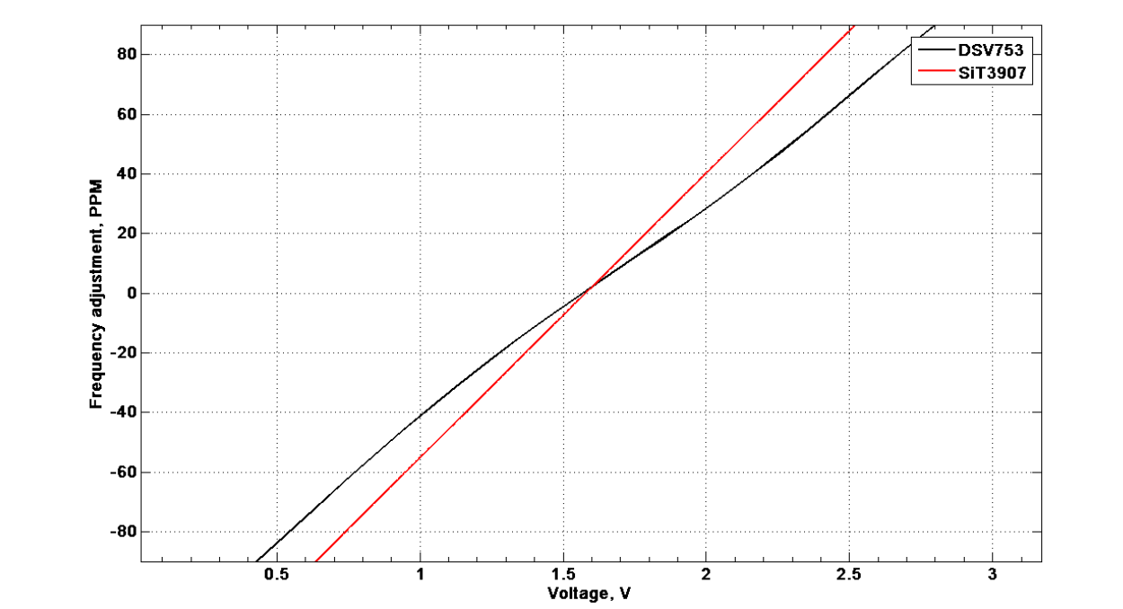
Figure 4: Linearity of a ±200 ppm PR DCXO, SiT3907 and ±90 pmm VCXO, DSV753SV.
As shown in Figure 4, kv of the VCXO exhibits non-linearity deviation when passing through the center of the tuning span and more linearity at the edges of the tuning span. The linear fit, built from the DSV753SV data, resides straight on the SiT3907 line (red colored). The DCXO nonlinearity is extremely low. Figure 5 shows frequency linearity of SiT3907AC-C3-33NZ-27.000000 with ± 1600 ppm PR across the full pull range. Measurements were taken with frequency pull register values from 0x000000 to 0x7FFFFF with the device operating in 23-bit mode (Mode 2). More details on DCXO modality in sec 3.2.
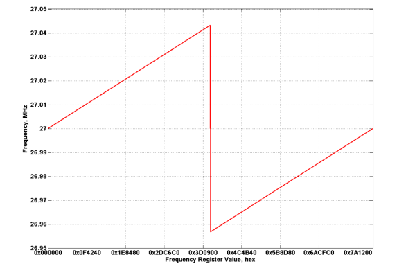
Figure 5: Frequency vs. “pull” register values for a SiT3907, 27 MHz, ±1600 ppm PR, Mode 2.
The SiT39xx pull frequency register value is represented as a two’s complement number for negative frequency shifts.
2.2 Phase Noise
Phase noise is a critical performance parameter of oscillators. For quartz-based VCXOs, manufacturers compromise between phase noise and PR. To achieve higher PR, a more “pullable” quartz crystal resonator is used which results in a lower Q-factor and hence higher phase noise.
The SiT39xx family of DCXOs does not suffer from this limitation. A designer can choose any of the offered pull ranges from ±25 ppm to ±1600 ppm without compromising phase noise performance. Phase noise plots of a SiT3907AC-C2-33NB-25.000000 (PR: ± 50 ppm) DCXO and SiT3907AC-C2-33NZ-25.000000 (PR: ± 1600 ppm) DCXO measured with an Agilent E5052B source signal analyzer are shown in Figure 6.
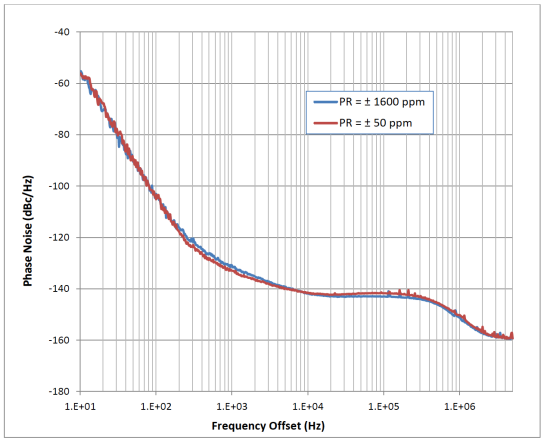
As shown in the above figure, the phase noise of the ± 50 ppm and ± 1600 ppm SiT3907 DCXO across the entire frequency offset range are within a dB.
3 Configuring SiT39xx DCXOs
3.1 1-wire Programming Interface
The SIT39xx family uses a proprietary 1-wire tri-level serial interface that can be simply implemented with minimum system resources: a tri-state capable GPIO pin either on an FPGA or an MCU. If the GPIO does not support tri-state output, two IOs may be used in combination with an external tri-state buffer (SN74LVC1G126) as shown in Figure 7.
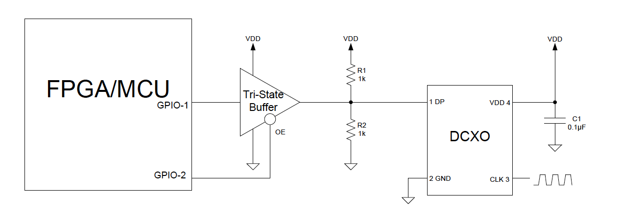
Figure 7: Serial 1-wire tri-level signaling
This SiTime Tri-level One-wire interface will be referred to by the acronym SiTLOWI. The signal levels of the SiTLOWI interface is shown in the waveform of Figure 8. The rise/fall time is determined by the RC time constant of the total capacitance at pin 1 (DP) and the parallel resistance of the pull-up and pull-down resistors. A logical bit “1” is defined by a high-logic followed by mid-logic level. A logical bit “0” is defined by a low-logic followed by mid-logic level. The waveform parameters are shown in Table 1. The time constant in most practical situations will be less than 50 ns; this necessitates choosing longer T_middle to allow the RC waveform to settle to within 5%. The captured waveform at the output of the tri-state buffer is shown in Figure 8.
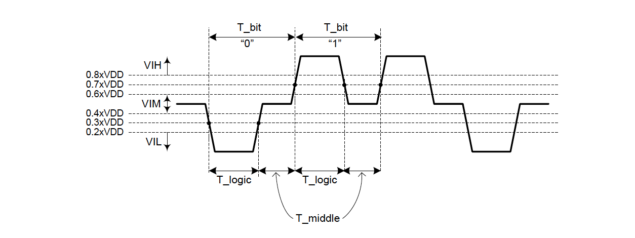
Figure 8: 1-wire programming interface waveform
Table 1: AD and DC parameters of 1-wire programming interface
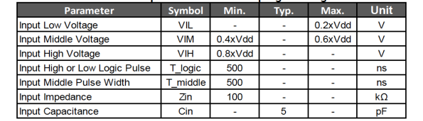
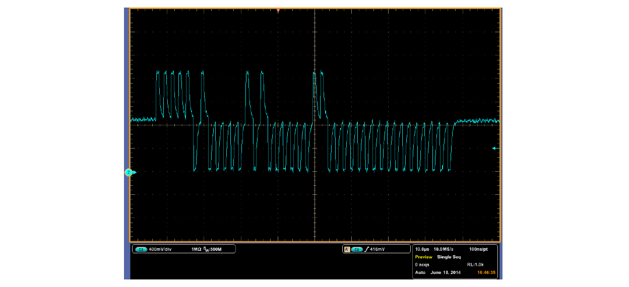
Figure 9: Captured data pin waveform
SiTime provides example C and HDL reference code to implement the 1-wire SiTLOWI interface with either an MCU or an FPGA.
3.1.1 Interfacing with an MCU
The MCU implementation is organized as open source native C API functions and supports simultaneous connections with up to 16 SiTime devices at 1 Mbit/s baud rate. This API can be easily integrated into any firmware of an 8/16/32-bit MCU. The SiTLOWI driver structure is illustrated in Figure 10.
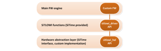
Figure 10: SiTLOWI driver structure
The example MCU API functions support the SiTLOWI implementation with and without an external tri-state buffer. The source code package is available on the SiTime website.
3.1.2 Interfacing with an FPGA
SiTime provides HDL code to implement the SiTLOWI master or transmitter interface on a Xilinx FPGA. This example code is written to be portable to other FPGA platforms. The design supports both a tri-state capable I/O pin or two IO pins with an external tri-state buffer. The design available in both Verilog and VHDL supports simultaneous connection with up to 16 SiTime devices at 1 Mbit/s baud rate. The transmitter high level block diagram is illustrated in Figure 11 The source code is available on the DCXO transmitter core specification webpage.
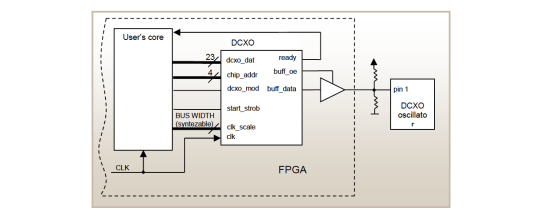
Figure 11: SiTLOWI Master/Transmitter block diagram.
3.2 Frequency Control
SiTime SIT39xx DCXO frequency is controlled via a set of two frequency “pull” registers which control the frequency shift from the device nominal frequency. Data for each register is written to the device using one data frame described in the following section.
3.2.1 Data Frame Format
Each frame as shown in Figure 12 consists of 40 bits. A frame has 3 parts:
1. The header, 16 bits, 0xFAXA, where X is the device address
2. Register address, 8 bits
3. Pull frequency (PF) value represented as two's complement binary number, 16 bits or 23 bits depending on programming mode explained farther. The value is split into two registers: MS Word value (address 0x06) and LS Word value (address 0x07)
The most significant bits are sent first.

Figure 12. Data frame format
The header allows the devices to recognize that the master is initiating communication. Field [7:4] of the header carries the device address that is factory programmable. The valid address value can be a hex digit from 0 to F. If not specified at ordering time, the device address will be defaulted to zero. For all examples in this document, the device address is considered to be zero (default).
3.2.2 Modes of Operation
The SiT39xx DCXO family supports two modes of operation. In mode 1, the user can control the device frequency by programming a 16 bit frequency “pull” value to register at address (0x06). In mode 2, the user can set a 23-bit ‘pull’ value by writing to 2 registers (0x06 and 0x07) to achieve higher resolution while maintaining a wide pull range. To access each of the registers, one data frame must be used.
3.2.2.1 Frequency Control Mode 1
In this resolution mode, only one frame per frequency update is required and the output frequency is updated at the end of each frame record. The length of the pull frequency data is 16 bits and is written to the device as shown in Figure 13.

Figure 13: Data format of frequency control Mode 1
The new frequency register value causes frequency update that will be performed after Tfdelay time; Table 2 lists the min/max values for this and other frame timing parameters. To reach the highest update rate, the next frame must be sent after 2 μs (Tf2f).
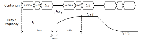
Figure 14: Mode 1 frame timing
Table 2: Frame Timing Parameters
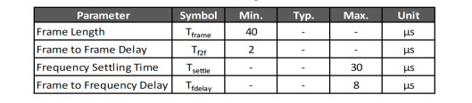
The device is ready to receive data after it goes through a valid powered up cycle. Frequency update does not lead to any interruptions of output oscillations. The frequency will switch from one value to the new value smoothly as shown in Figure 14. Figure 16 shows a scope snapshot of the frequency trend (purple) after a code sequence adjusts the frequency from -1600 ppm to +1600 ppm.
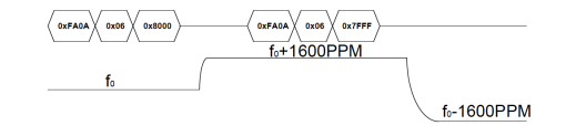
Figure 15: Trend of frequency Transition in Mode 1
Figure 16. Scope snapshot of frequency update from -1600 ppm to +1600 ppm in Mode 1.
3.2.2.2 Frequency Control Mode 2
In this mode, two frames per frequency update are required and frequency is only updated at the end of the second frame. The pull frequency value in this mode is 23 bits. This mode provides better step resolution. This value is written to the device in two frames as shown in Figure 17. The first frame carries 7 LSB of the LS word value (address 0x07). The rest of the most significant bits in register 0x07 must be set to 0. The second frame carries 16 bit of the MS word value. Frame timing waveform for this mode is shown in Figure 18.
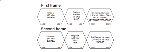
Figure 17: Data format of frequency control Mode 2
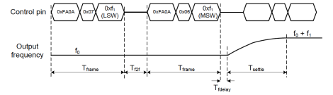
Figure 18: Mode 2 frame timing
3.2.2.3 Calculating Frequency Pull value
There are a few steps to calculate the correct frequency value of SiT3907:
1. Find the scale factor from the table below where PR is the Pull Range (1600 ppm, 800 ppm etc.):
- Mode 1: (2^15-1) / (PR*1.00135625)
- Mode 2: (2^22-1) / (PR*1.00135625)
2. Enter the desired_PPM value in equation: Frequency control (decimal value) = round (abs (desired_PPM * K))
For any positive frequency shift, write the value either to the register or to the registers depending on the chosen mode. For negative frequency shift values, convert to a two’s complement binary number and write to the registers.
3.2.2.3.1 Example 1. Calculating frequency shift for Mode 1
To calculate +120.3 ppm frequency shift in Mode 1 (16-bit) for the device (address 0) with the ±1600 ppm PR, find the decimal value that can be calculated as mentioned above.
1. Find the scale factor:
K = (2^15-1)/(1600*1.00135625) = 20.451637…
2. Calculate the pull frequency value:
Round (120.3 * K) = 2460
3. Since, we have positive frequency shift, the value is used as hexadecimal number that will be written to the pull frequency register:
2460 = 0x099C
The data frame to be written to the device is 0xFA0A 06 099C.
3.2.2.3.2 Example 2. Calculating Frequency Shift for Mode 2
Mode 2 (23-bit) requires two words to be written to set the desired frequency shift. If negative frequency shift is -920.2 ppm for the same device, the same procedure to calculate the pull frequency value is used.
1. Find the scale factor:
K = (2^22-1)/(1600*1.00135625) = 2617.8888…
2. Calculate decimal value of the frequency register:
Round (920.2 * K) = 2408981
3. Negative frequency shift has to be converted to the two’s complement value that will be written to the frequency register
23-bit hexadecimal value: 2408981 = 0x24C215
23-bit two’s complementary hexadecimal value: 0x24C215 = 0x5B3DEA
4 Conclusions
The SiT39xx family of DCXOs features high linearity with high stability and lower phase noise. These DCXOs offer sufficiently high update rate and resolution to minimize the quantization impact on close-in phase noise, and are suitable for implementing an all-digital low bandwidth PLL, which eliminates additional overhead related to analog circuitry.
DCXOs offer several key advantages over VCXOs:
- Extremely linear characteristic. Linearity better than 1% is easily achieved as compared to 5% to 10% obtained through varactors used in VCXO architecture
- User-programmable kv
- No trade-off between kv and APR
- No degradation of close-in phase noise due to input circuit analog noise
- No trade-off between pull range and phase noise
- No additional circuitry for digital-to-analog conversion or bulky analog filters
- 8x wider pull range compared to standard VCXOs
- Superior tuning slope (kv) consistency minimizes variation in system PLL performance and simplifies PLL design