Analysis of High-stability Controlled Oscillators for Low-bandwidth PLLs
Sassan Tabatabaei, stabatabaei@sitime.com
SiTime Corporation www.sitime.com
990 Almanor Avenue, Sunnyvale, CA 94085
Abstract
For low bandwidth PLLs, high-Q controlled oscillators (CO) are the devices of choice due to their low gain and high stability. This paper discusses two different implementations of voltage-controlled oscillators (VCXOs), varactor-based and PLL-based. It also discusses digitally-controlled oscillators (DCXOs) to increase flexibility and robustness in system design while considering the impact of quantization, update delay, and loop filter implementation on the loop performance.
1. Introduction
High stability controlled oscillators (CO) are used in synchronization or jitter clean-up PLLs for networking, telecom, video/audio, and instrumentation applications. Such PLLs typically have very low bandwidth e.g., less than 1 kHz, to filter out much of the phase noise and jitter from the reference input clock. These circuits use high-Q mechanical resonators to achieve very low frequency control gain and high stability, which are necessary for design of stable low-bandwidth PLL. The two main high-stability controlled oscillators are as follows.
- Voltage-controlled oscillators based on pullable high-Q resonators (VCXO)
- Digitally-controlled oscillator based on high-Q resonators (DCXO)
The native frequency stability of either VCXO or DCXO can be improved for applications that require very stringent stability when the input to the PLL is interrupted and the controlled oscillator is effectively free running. Examples include synchronizers and retimers in SONET and telecom applications with holdover features. In such cases, the mechanical resonator frequency is further stabilized through temperature compensation techniques (VC-TCXO or DC-TCXO) to correct for frequency variations over temperature or oven-controlled techniques (VC-OCXO or DC-OCXO) to stabilize the resonator temperature and avoid frequency variation based on changes of ambient temperature.
Most widely used high-Q resonators are based on either quartz crystal or micro electromechanical system (MEMS) resonators [1]. These resonators rely on mechanical properties of quartz crystal or silicon material, respectively, to achieve high Q. Quartz resonators operate based on a piezoelectric phenomenon. These resonators generate maximum current when mechanical stress is applied to them at their resonance frequency. In contrast, the current commercially available MEMS resonators use electrostatic excitation to generate high-Q oscillation [1].
High stability COs use two main methods for frequency control as listed below.
- Pull the mechanical resonator frequency directly
- Pulling using high resolution PLLs
The above frequency-controlled devices provide different features and benefits, which impact the design and performance of low-bandwidth PLLs that use them. This paper analyzes these features and benefits and examines the resulting trade-offs.
2. VCXO Architectures and Specifications
Before explaining the architecture and features of different types of VCXOs, let us define key VCXO specifications as below.
Pull range (PR)
The frequency control range for the full input voltage range under nominal conditions.
Absolute pull range (APR)
The guaranteed frequency control range under the full range of operating conditions, including temperature, aging, and voltage/load variations. APR is computed as PR minus the oscillator frequency stability due to any other factor.
VCO gain (kv)
The ratio of frequency variation for a given input voltage variation. This ratio is expressed as Hz/V or ppm/V.
Close-in phase noise
The phase noise at frequency offsets below 10 kHz offset, which is typically dominated by the input voltage noise sensitivity
2.1 VCXO Architectures
VCXOs use one of the two frequency control methods listed below.
1. Pull the mechanical resonator frequency directly
A common example of this type of VCXO is a quartz-based oscillator with resonance frequency controlled by changing the shunt capacitances. Typically, capacitance is controlled with a voltage using varactors, yielding VCXO devices. This example is shown in Figure 1.
2. Pulling using PLLs
In this architecture, the stable oscillator output drives a high-resolution PLL, typically a fractional-N PLL to achieve sufficiently high resolution. The PLL modulator is driven in analog fashion using an analog-to-digital converter (ADC). This architecture is shown in Figure 2.
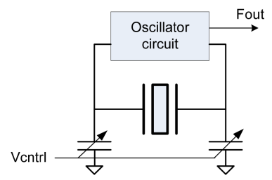
Figure 1: VCXO based on pulling the resonator frequency
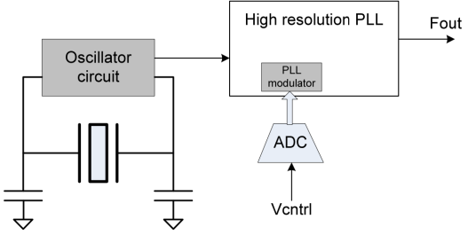
Figure 2: VCXO based on non-pullable resonator and high resolution PLL
2.2 Varactor-based VCXOs
These VCXOs use varactors to “pull” the frequency of a quartz-based oscillator and have been widely used in many applications. Their usage, however, requires careful trade-off of noise, APR and Kv. Typically, it is better to choose lowest Kv for a target APR to minimize the phase noise impact and improve PLL stability. Accommodating pull ranges wider than +/-100ppm may adversely impact the phase noise performance or reliability/quality of the devices. The Kv linearity versus control voltage is in the 10% range, which impacts the PLL bandwidth and stability over full operating range.
2.3 PLL-based VCXO
PLL-based VCXOs use a high-resolution PLL driven by a high-stability oscillator, such as MEMS- or quartzbased oscillators, as shown in Figure 2. The frequency control function is implemented through an ADC that digitizes the input voltage and drives the fractional-N PLL modulator. This architecture offers the following advantages.
- Kv linearity of 0.1% to 1% is easily achievable
- Wide pull ranges (>1000pm) can be achieved without compromising the quality of MEMSor quartz-based oscillators
Such VCXOs, however, do require additional ADC and fractional-PLL circuits. The ADC digital resolution is typically designed to be less than the thermal noise of the AC circuit. The ADC is followed by a low pass filter to minimize the thermal and quantization noise. The overall circuit allows effectively infinite resolution due to the dithering effect of thermal noise. Therefore, from the application point of view, there is no difference between direct analog control and using such ADC in terms of frequency control resolution.
The effect of ADC noise on the close-in phase noise depends on the pull range. The higher the pull range, the more sensitive the output is to the input noise. For low pull range, in the range of ±50ppm or lower, the noise impact is typically minimal, meaning the close-in phase noise is mostly dominated by the oscillator phase noise.
The Vin noise impact increases proportionally to the pull range, roughly 6 dB for every doubling of pull range. This is also true for varactor-based quartz VCXOs. Therefore, there is a trade-off between close-in phase noise and pull range in both types of VCXOs.
3. VCXOs in Low Bandwidth PLLs
Low-bandwidth PLLs can be implemented in two major ways:
- Use a phase detector and/or charge-pump followed by very low bandwidth analog loop filter as shown in Figure 3. The loop filter R and C values typically are very large due to low bandwidth.
- Use a phase detector with digital output. Implement the loop filter in the FPGA and use a digital-to-analog converter (DAC) to drive the VCXO as shown in Figure 4.
The second approach is more flexible because the filter can be modified easily through software. However, it requires additional DAC circuitry, which can be a simple pulse width modulator (PWM) circuit followed by an resistor-capacitor (RC) filter.
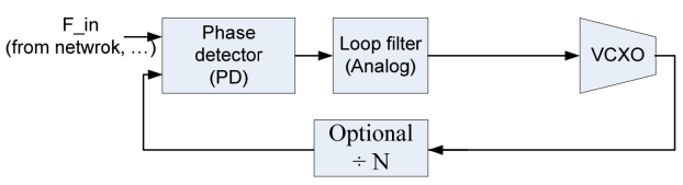
Figure 3: Low bandwidth PLL with VCXO and analog loop filter
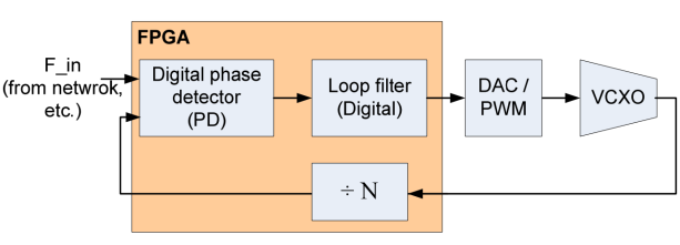
Figure 4: Low bandwidth PLL with VCXO and digital loop filter
4. DCXO Architecture
DCXOs can also be implemented in two ways.
- Pull a quartz resonator frequency by switching a series of shunt capacitances digitally as shown in Figure 5.
- Use high resolution PLL slaved to a high-Q oscillator. As shown in Figure 6, the frequency control function is achieved by directly driving the digital input of the PLL feedback divider or fractional-N PLL modulator.
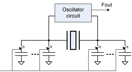
Figure 5: DCXO based on resonator pulling
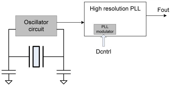
Figure 6: DCXO based on high-resolution PLL
The DCXO allows maximum flexibility in optimizing key controlled oscillator parameters. The advantages of DCXO in low bandwidth PLL are:
- Extremely linear characteristics. Linearity better than 1% is easily achievable as opposed to 5% to 10% obtained through varactors
- User-programmable Kv
- No trade-off between Kv and APR. The pullable resonator tends to become less stable over temperature. This requires greater pull range and Kv to achieve the target APR
- No degradation of close-in phase noise due to input circuit analog noise
- No trade-off between pull range and phase noise
- No additional circuitry for digital-to-analog conversion or on-board analog filters
Additionally, DCXOs allow dynamic control of loop bandwidth using an FPGA or microcontroller (uC). For example, bandwidth can be set higher to reduce locking time and then reduced to improve the tracking dynamics and stability.
Designing with DCXOs, however, requires attention to issues that are not relevant when using VCXOs.
5. Using DCXOs for Low Bandwidth PLLs
The output frequency of a DCXO is controlled by writing to some internal registers of the device. The characteristics of DCXO that need to be considered in a PLL design are as follow.
- Frequency control resolution
- Frequency update rate
- Frequency update delay
The combination of frequency resolution and update rate determines the additive phase noise due to quantization noise. Figure 7 shows the simulated results for close-in phase noise for a 10 MHz DCXO for different resolutions. This simulation assumes that the update rate is 25000 update/s. As this figure illustrates, the additive phase noise starts dominating at frequency offsets below 10 kHz with 100 ppb (1e-7) DCXO resolution. The impact of DCXO quantization noise is below or slightly higher than the native phase noise of most MEMS-based or quartz oscillators for the resolution of 10 bbp (1e-8). At this level, the DCXO quantization noise has little impact on the phase noise performance. Today’s modern DCXOs, such as the high-precision SiT3907 from SiTime [2], easily provide 1 ppb or better resolution, which effectively eliminate any quantization impact on output phase noise.
The update rate can also be an important contributor to the final phase noise. Typically, low update rate causes the error signal from the phase detector and loop filter to be integrated by the DCXO for a long time, which results in higher phase noise. The simulations in Figure 8 show the effect of update rate for a DCXO with resolution of 1 ppb. This simulation shows that even update rate in the range of 2500 update/s is sufficient to ensure the quantization noise does not affect the overall phase noise.
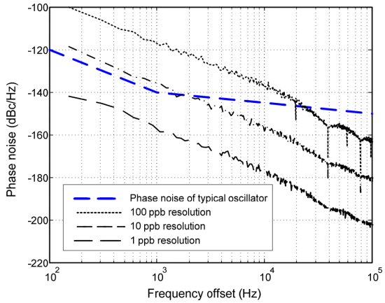
Figure 7: Quantization-induced phase noise for different frequency DCXO control resolutions
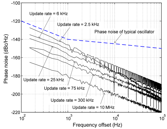
Figure 8: The effect of DCXO update rate on close-in phase noise
The low bandwidth PLL stability also needs to be considered when using DCXOs. In addition to the loop filter response, the update rate and delay of the DCXO contribute to the overall stability of the loop. For a guaranteed stable operation, typically the update rate and inverse of the update delay should be at least 10 times higher that the target loop bandwidth. This means that for a 1 kHz loop bandwidth, the update rate should be higher that 10 kHz and the update delay shorter than 100 us. Fortunately, DCXOs that can support such specification are available from multiple sources [2]. The DCXO output frequency can be controlled with discrete steps. That leads to the question of what the frequency error will be once the PLL loop is in lock condition. This is related to the DCXO resolution and update rate. Effectively, the low bandwidth PLL loop will result in a Gaussian noise at the input of the DCXO.
The DCXO averages this noise. The frequency error can be computed as the quantization noise at the input of the DCXO divided by the square root of the number of times the frequency errors are averages. For example, for a DCXO with resolution of 1 ppb and update rate of 25000 update/s, the quantization-induced frequency error over 1s interval is: 1ppb/sqrt(25000)=0.006ppb.
Over longer time intervals, the frequency error decreases even more. This low level of frequency error allows the use of such DCXOs in demanding applications such as telecom where very tight frequency locking is required.
Another implementation issue when using DCXOs is the choice of phase detector. Two attractive options are:
- Use a high-speed phase detector (PD) that can operate at the output frequency rate
- Divide the input and output paths to the phase detector and use a low-speed phase detector
In ether case the PD is followed by the digital loop filter. In first option the output of the PD needs to be digitized and passed to the filter. Although the number of bits required from the digitizer is not high, it has to operate at a fairly high rate. The second option allows use of a slower digitizer which may be easier to implement. In this case the digitizer rate has to be at least 10 times higher than the loop filter bandwidth to minimize impact on loop stability.
6. Conclusion
The PLL-based VCXOs and DCXOs provide advantages in pull range and flexibility, although they require carefully designed high resolution PLLs. More specifically, the DCXOs allow flexible fully-digital implementation of low bandwidth PLLs for high performance synchronization and jitter cleaning. Today’s DCXOs offer sufficiently high update rate and resolution to ensure any quantization impact on close-in phase noise can be safely ignored.
References
[1] S. Tabatabaei, et. al, “Silicon MEMS Oscillators for High-Speed Digital Systems”, IEEE Micro, vol. 30, No. 2, March/April 2010, pp 80-89.
[2] SiTime Corp., “High Precision Digitally Controlled MEMS Oscillator”, SiT3907 Datasheet