Content
2.1 PLL as a frequency tracker/filter
3. Effects of VCXO parameters on PLL performance
3.1.1 Benefits of SiTime VCXOs for Absolute Pull Range
3.3.1 Benefits of SiTime VCXOs for Kv Variation
1 Introduction
Many VCXOs are key components in low-bandwidth PLLs. Such PLLs are often used for synchronization and/or jitter cleanup in telecom, video, audio, networking, and instrumentation applications. This application note describes the relationship of the key VCXO-specific performance parameters and their tradeoffs in PLL design.
2 Basic PLL architecture
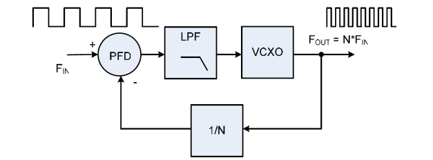
Figure 1: Typical PLL Block Diagram
Figure 1 shows a simple PLL block diagram. A reference clock supplies an input frequency, FIN. A Phase Frequency Detector (PFD) compares the phases of the input clock and the output clock, and generates a periodic error signal based on the phase difference. This periodic signal is low-pass-filtered through a loop filter (LF), and passed as an analog control voltage to the VCXO input.
The VCXO output frequency is controlled by, and roughly proportional to, the control input voltage. The output frequency will vary with changes in the control voltage, until the resulting phase error energy is driven to zero. In the common case shown above, there is a divide-by-N between the output frequency generated by the VCXO, and the frequency fed back to the PFD. This results in an effective multiply-by-N of the reference frequency.
2.1 PLL as a frequency tracker/filter
The PLL output tracks variations in the reference frequency as long as the speed of the variations is within the overall bandwidth of the PLL loop filter. It also smooths out, or filters, high-frequency variations, or jitter, in the input reference frequency. This is an example of using the PLL as a “jitter cleaner” – tracking low-frequency variations in a reference clock, for example in a network-synchronization application, while filtering out high-frequency jitter.
A tradeoff here is that low-frequency offset phase noise in the VCXO itself is also attenuated, and high-frequency offset VCXO phase noise is passed through to the output. So the same loop that acts as a low-pass filter for reference input noise acts as a high-pass filter for VCXO noise. In such a design, there is a tradeoff in selecting the loop bandwidth for several conflicting goals:
- Attenuating reference input noise (lower bandwidth is better)
- Tracking reference variations up to a desired bandwidth (higher tracking speed requirements means higher bandwidth)
- Attenuating VCXO-generated noise (higher bandwidth is better).
The first two of these goals are equivalent to the usual tradeoff in a low-pass filter: tracking performance vs. noise filtering performance. In general, using a lower-noise VCXO eases the tradeoff of these two parameters, as attenuating the VCXO-generated noise is less of a consideration.
The VCXO in the PLL system can usually be modeled as a simple gain Kv [1]. As with any feedback system, the closed-loop dynamics will be a function of this gain, and may be become unstable due to poor choices of Kv. Kv is therefore one of the more critical choices in loop design. Suitable ranges of Kv are usually dictated by the application’s requirements, and limited by the availability of VCXO parts that can meet these requirements.
3 Effects of VCXO parameters on PLL performance
In PLL design, tpically minimum Kv and maximum APR is desired. However, it is difficult to obtain both at the same time with Quartz-based VCXOs. This section describes the tradeoffs between APR and Kv, and explain how SiTime VCXOs relieve the designer from making such tradeoffs.
3.1 Absolute Pull Range
Since the PLL designer is usually concerned about tracking a specified range of input frequencies over all conditions, Absolute Pull Range (APR) [1] is a more relevant specification for PLL design.
Figure 1 shows frequency vs. voltage (FV) characteristics for both a typical quartz VCXO and a SiTime VCXO. The grey bands illustrate how far the FV characteristics can vary with conditions, and demonstrate the difference between nominal, or total, pull range, and APR. The APR must be larger than the maximum expected reference frequency variation. Otherwise, the PLL may not be able to track the reference input frequency.
For quartz-based VCXOs, to get a higher APR it is usually necessary to use a lower-Q crystal to make the crystal more “pullable.” However, this also has the effect of degrading frequency stability. Therefore, a tradeoff must be made between the minimum APR required by the application, and the minimum frequency stability available with that APR. Generally, it is best to choose the lowest APR that meets the application’s requirements.
3.1.1 Benefits of SiTime VCXOs for Absolute Pull Range
Since a higher pull range VCXO usually implies larger (worse) frequency stability, it is not unusual to select a VCXO with a nominal pull range significantly larger than would be otherwise required, just to provide a high enough APR to meet minimum application requirements. This usually carries design penalties by requiring VCXOs with steeper FV characteristics, which can adversely affect noise and stability margins in a PLL design.
SiTime’s VCXO families are not subject to this effect. Because the frequency change in response to control voltage change is generated through a PLL within the VCXO device, SiTime has made the frequency stability independent from the pull range itself. This allows a designer to select exactly the APR required by the application, and no more.
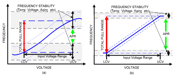
Figure 2: Typical VCXO FV characteristics: (a) Typical Quartz VCXO characteristics, (b)Typical SiTime VCXO characteristics
3.2 Kv Linearity
The Kv [1] of a standard quartz-based VCXO may vary significantly over the input control voltage range, typically from 10 to 20%. Generally, a part with better linearity specifications will have a lower variation in Kv, but it is possible to have a significant variation in Kv even in parts with a good linearity specification.
Some datasheets may specify an “average” Kv, but since Kv affects important PLL performance parameters such as bandwidth and phase margin (stability), the entire Kv variation must be understood and accounted for in a successful design.
3.3 Kv effects on PLL design
For most low-bandwidth PLLs, the VCXO’s FV characteristic is modeled as the simple gain, Kv. As with any control system, adjusting the gain will change the closed-loop dynamics. In the vast majority of cases, increasing Kv will increase loop speed (better tracking), but will also increase overshoot and peaking, and may drive the closed-loop system closer to instability. A higher Kv will also make the system more sensitive to voltage noise at the control input, increasing overall system jitter.
Typical quartz-based VCXOs achieve their voltage-control function via a varactor, which leads to a curved FV characteristic, as shown in Figure 3(a). Linearity specifications for these devices are typically in the range of 5 to 10%. This curved characteristic can lead to a Kv characteristic that varies significantly over the input voltage control range, as shown in Figure 3(c). To use such a VCXO successfully, a PLL designer must account for both the minimum Kv, which limits PLL bandwidth and tracking ability, as well as the maximum Kv, which dictates worst-case jitter and noise performance, and worst-case system stability.
To compound matters, the linearity and Kv curves themselves may shift with conditions such as temperature and Vdd, forcing the designer to account for the worst-case effects of these conditions on Kv. These dependencies may not be well documented on a given datasheet, but may only be captured in conservative “min” and “max” Kv specs.
Finally, a designer may initially select a VCXO family on the basis of minimum APR. Because the frequency stability of the VCXO gets worse with higher APR, a higher Kv is necessary to achieve the same APR over the same voltage control range. This means that the Kv may need to be selected significantly higher than is required for system performance and loop stability, simply to meet an APR specification!
3.3.1 Benefits of SiTime VCXOs for Kv Variation
For comparison, Figure 3(b) and Figure 3(d) show the linearity and Kv variation of SiTime’s 380X series VCXOs. The FV characteristic is extremely linear, typically much less than 1%, and the Kv will remain extremely constant throughout the control range.
Furthermore, in the SiTime design, frequency stability and Kv are specified as totally independent quantities. This means that designers are free to independently choose exactly the frequency stability, APR, and Kv that are appropriate for their applications. Additionally, since the Kv remains constant across the entire control voltage range, there is little need for worst case analyses which consider large Kv variations over conditions. All of these benefits together significantly reduce the burden on the PLL designer.
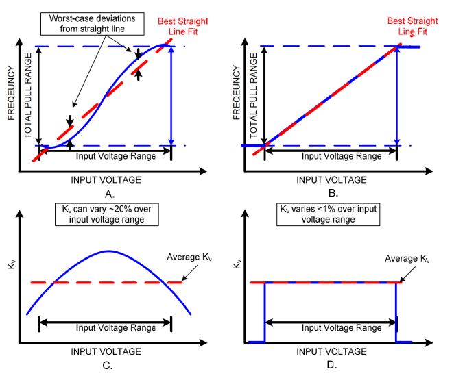
Figure 3: VCXO linearity and Kv characteristics: (a) Typical quartz VCXO FV characteristics, (b) Typical SiTime VCXO FV characteristics, (c) Typical Quartz VCXO Kv variations, (d) Typical SiTime VCXO Kv variations
4 Conclusion
This document has illustrated some of the most important VCXO performance specifications and their application to one of the most important VCXO applications, PLL design. It has also illustrated some of the important differences in these specifications between legacy quartz VCXOs and SiTime VCXOs, and the benefits that SiTime VCXOs can provide to PLL designers in terms of reduced need to trade off critical parameters such as APR, Kv and frequency stability.