How to Evaluate Reference-Clock Phase Noise in High-Speed Serial Links
Most high-speed serial-data communications standards do not include specifications for reference-clock (refclk) jitter. Instead, jitter is specified for the serial-data signal, a portion of which originates from the refclk. Thus, these standards limit refclk jitter indirectly. Such a scheme gives designers more freedom to choose refclks, and budget jitter accordingly.
Traditionally, real-time oscilloscopes have been used to determine jitter compliance in serial-data signals. This analysis is straightforward because an oscilloscope-based time-interval error (TIE) jitter measurement observes jitter similar to an actual system, whose jitter filtering may be emulated in software executed in the oscilloscope.
On the other hand, clock-jitter analysis traditionally derives jitter from a phase noise analyzer due to its inherently lower instrument noise floor. Since an oscilloscope and phase noise analyzer observe jitter differently, obtaining the same value from both instruments can be challenging. This article presents a phase noise based methodology that provides similar values as TIE jitter derived from an oscilloscope, and therefore the actual system. This methodology is used by PCI Express® BASE Specification Revision 5.0 for refclk jitter compliance. An expanded version of this article is available online at Signal Integrity Journal. 1
HOW PLLs OBSERVE PHASE NOISE
A phase-locked loop (PLL) is a basic building block in many digital and RF systems. Figure 1a shows an example PLL whose phase detector compares corresponding input and feedback edges, and outputs a pulse proportional to their phase difference, which is then filtered to control a voltage-controlled oscillator. In this example, the phase detector samples its inputs at their rising-edge midpoints. Therefore, the average sampling (FS) and input clock frequencies (FIN) are equal.
Spectral components of jitter located above the Nyquist frequency (FS/2) alias, or fold back, below the Nyquist frequency after sampling. Figure 1b illustrates the PLL jitter transfer function, whose lowpass filtering characteristic is mirrored across spectral boundaries at integer multiples of the Nyquist frequency, FS/2. Below the Nyquist frequency, jitter frequencies falling inside the PLL loop bandwidth pass unattenuated, whereas jitter frequencies falling outside this bandwidth get attenuated by the response of the loop. Figure 1c uses a logarithmic x-axis to plot a similar transfer function for a PLL having a closed-loop bandwidth of 5 MHz. The plot is drawn arbitrarily to 1 GHz.
Figure 2 illustrates how phase noise in a 100 MHz input clock signal gets filtered by an example PLL2 with a closed-loop bandwidth of 1 MHz. The green “Filter” curve shows the jitter transfer function of the PLL up to an arbitrary offset frequency of 500 MHz. Note that the x-axis represents frequency offset from the carrier, as appropriate for phase noise, so that a 500 MHz offset on the x-axis would appear at 600 MHz in the signal spectrum (e.g., 500 MHz offset plus 100 MHz carrier). The 100 MHz input signal’s phase noise is also shown in Figure 2 using a black curve labeled “Raw Data.” Adding the Filter and Raw Data curves produces the blue “Filtered Data” curve, which represents how much of the input signal’s phase noise passes through the PLL to appear in the output signal. The filtered phase noise curve can then be integrated over an offset-frequency range of interest to convert it to jitter.3
However, a few issues complicate this integration. First, the Raw Data curve shown in Figure 2 is not possible to measure at high offset frequencies. A phase noise analyzer measures phase noise directly, but it can only measure up to an offset frequency equal to a fraction of the fundamental clock frequency. The Raw Data curve drawn in Figure 2 is thus for illustration only. In reality, phase noise in a 100 MHz clock signal can only be directly measured up to a maximum offset frequency of 30 or 40 MHz, depending on the instrument.
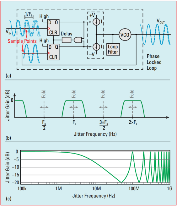
Fig. 1 Phase locked loop (a) block diagram illustrating sampling at the phase detector,
and example jitter-transfer function with (b) linear and (c) logarithmic x-axis.
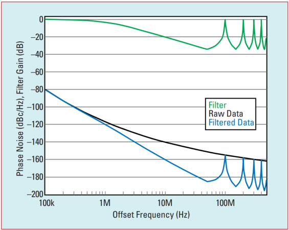
Fig. 2 Illustration of phase noise in a 100 MHz input clock aliasing in a PLL by adding a PLL jitter-transfer
function (green) to the input phase noise Raw Data (black) to derive an output Filtered Data phase noise (blue).
Phase noise at higher offset frequencies can be estimated using a spectrum analyzer. However, since a spectrum analyzer cannot distinguish between phase and amplitude noise, any spectrum analyzer analysis of phase noise assumes that phase noise dominates at all offset frequencies. When this is not true, accuracy degrades, which may cause the result to be optimistic or pessimistic depending on several factors.4 For precision clock sources, phase noise usually dominates at near-in offset frequencies. Amplitude noise and/or modulation may dominate further out.
Secondly, before the filtered phase noise can be integrated, the integration limits must be identified. The lower integration limit is typically set by the application, such as the bandwidth of a receiver’s observed jitter transfer function. The upper integration limit should extend until the phase noise falls to an insignificant level. One might assume this occurs near the analog input-bandwidth of the phasedetector block in the transmit SERDES PLL.
For example, if the phase-detector’s analog input bandwidth is 600 MHz, then the filtered phase noise curve should be integrated to a 500 MHz offset (e.g., 600 MHz analog bandwidth minus a 100 MHz carrier equals 500 MHz offset frequency). However, a signal’s measured phase noise is independent of its amplitude, at least until its amplitude approaches the instrument’s noise floor. Thus, to first order, the input signal’s phase noise is not influenced by the analog input bandwidth of the phase detector, as the signal passes through the PLL.
These issues make it difficult to determine an upper integration limit for converting the filtered phase noise into jitter, which we will address below.
HOW SERIAL-DATA LINKS OBSERVE REFCLK PHASE NOISE
Knowing how input phase noise aliases when sampled by a PLL, we can now model the jitter-transfer function of a serial-data communications link. As an example, we will use the common-clock timing architecture used by PCI Express,5-6 as shown in Figure 3. Here, the refclk phase noise, X, is filtered by the transmit PLL jitter-transfer function, H1, and the receive PLL and CDR jitter-transfer functions, H2 and H3, respectively. Note that H3 is modeled for 32 GT/s links in Figure 3. The overall system jitter transfer function, Y, is a function of H1, H2, H3, and T, which is the refclk time delay between transmit and receive paths. The phase noise contribution from the reference clock that appears on the output data is therefore computed as X × Y.
PCI Express 5.0 at 32 GT/s requires filtering the refclk with 16 different system jitter transfer functions. The worstcase function, which leads to the highest jitter, for a given refclk is computed and plotted between 10 kHz and 30 MHz as the green Filter curve in Figure 4a. The raw measured phase noise data is also plotted in Figure 4a, as a black curve labeled Raw Data. Finally, the filtered phase noise data is computed by adding the Filter and Raw Data curves and plotted in Figure 4a as a blue curve labeled Filtered Data.
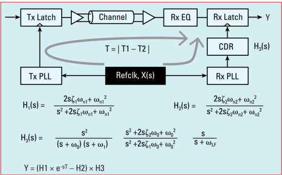
Fig. 3 Illustration of PCIe5 32 GT/s system jitter-transfer function (Y)
used to filter refclk phase noise (X) in a commonclock timing architecture.
A traditional PCI-SIG analysis evaluates TIE jitter in a 100 MHz refclk using a real-time oscilloscope. This method samples TIE jitter at each rising edge in the clock waveform, such that spectral components of jitter above the Nyquist frequency of 50 MHz alias below 50 MHz, as done in the real system. Therefore, a TIE jitter spectrum extends up to 50 MHz, and correctly aliases higher frequency components of jitter (as done in the real system).
By contrast, a phase noise analyzer includes a low-pass filter that prevents measuring phase noise up to an offset frequency equal to half the clock frequency (e.g., 50 MHz). It is therefore common industry practice7 to extend the last-measured phase-noise data point up to a 50 MHz offset frequency, to match the appearance of a TIE jitter spectrum. Figure 4a illustrates this practice by extending each of the three curves using red segments from 30 to 50 MHz.
The problem with this, is that a TIE jitter spectrum includes aliased components of jitter, whereas the phase noise spectrum shown in Figure 4a does not. To account for aliasing, Figure 4b uses (1) a red line to extend the last measured Raw Data phase noise data point to an arbitrary value of 2 GHz, and (2) extends the green Filter curve by mirroring it across spectral boundaries located at integer multiples of the Nyquist frequency (i.e., 50 MHz). The filtered phase noise data shown in Figure 4b as a blue curve labeled Filtered Data now accounts for aliased components of phase noise up to an offset frequency of 2 GHz. The filtered phase noise data can then be integrated to convert it to jitter.3
In performing this integration, we observe that the filtered phase noise below 100 kHz is sufficiently low that it can be ignored. However, the filtered phase noise around 2 GHz is significant and, in fact, dominates the integral. The result is, similar to the PLL analysis above, that we cannot define an upper-integration limit to derive jitter from the filtered phase noise. Further analysis is required.
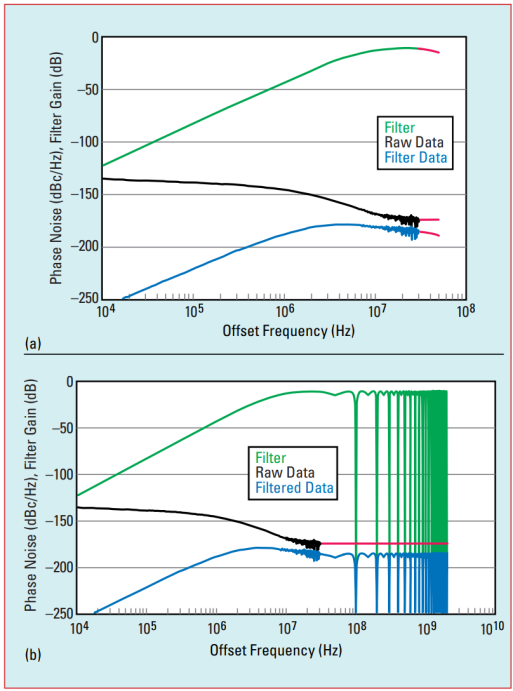
Fig. 4 Example phase-noise extensions that (a) do not account, and (b) do account for phase noise aliasing when sampled by a PLL.
MOTIVATION
Our goal is to find a method to derive jitter from phase noise that matches TIE jitter traditionally measured with an oscilloscope (without jitter added from the test environment). Since an oscilloscope observes jitter similar to a real system, we regard its result as the gold standard against which other methods may be judged (assuming the oscilloscope does not add a significant amount of jitter, or that it can be subtracted out during post processing). The rest of this article presents the conclusions from an exhaustive study8-9 to determine such a method3. The study analyzed nine different clock devices manufactured by four different companies. The devices were chosen to cover a wide range of jitter values, spanning two orders of magnitude.1
EMPIRICAL ANALYSIS
Empirically, we determined that the best match between phase noise analyzer and oscilloscope-based jitter measurements occurred when the phase noise analyzer data is extended as a flat line up to the third harmonic, and postprocessed as described above. Figure 5 illustrates a 100 MHz clock signal measured with a phase noise analyzer (black curves), before and after applying a system jitter filter. A flat green extension of this data is also drawn, up to a 200 MHz offset frequency (e.g., 300 MHz signal frequency, or third harmonic). For reference, spectrum analyzer data is shown in blue. If we assume the spectrum analyzer data represents phase noise, then the region that dominates the integral of the spectrum analyzer’s phase noise can be located by drawing a −10 dB/decade line above the curve and lowering it until it intersects the curve.10
The point of intersection identifies the dominant contribution to this integral, or jitter value. This intersection is observed to occur at the third harmonic in Figure 5. The phase noise spectrum rolls off significantly above the third harmonic and can be safely ignored. Below the third harmonic, the (green) flat phase noise extension partly overestimates and partly underestimates the true phase noise in the signal, balancing each other out. The resulting filtered phase noise with flat extension up to the third harmonic empirically provides a good match to traditional oscilloscope results for jitter.1
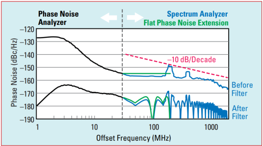
Fig. 5 Example 100 MHz clock phase noise, in which the integrated phase noise located beyond the phase noise analyzer measurement data
(e.g., 30 MHz) is dominated by the third-harmonic contribution (e.g., at 200 MHz offset frequency).
PHASE NOISE METHODOLOGY
The recommended methodology for analyzing phase noise in sampled systems may be summarized as follows, with reference to Figure 6.
- Measure a DUT’s raw phase noise in dBc/Hz using a phase noise analyzer (not a spectrum analyzer). A 100 MHz signal is illustrated in Figure 6.
- If needed, remove spurs to analyze random noise only.
- Extend the phase noise plot with a straight line up to twice the clock frequency (i.e., 200 MHz offset frequency, equivalent to the third harmonic, or 300 MHz, in the signal spectrum).
- Mirror the jitter filter across spectral boundaries located at integer multiples of the Nyquist frequency (e.g., 50 MHz), up to twice the fundamental clock frequency (i.e., 200 MHz offset frequency). Alternatively (not shown), alias phase noise data (from Step 3) located above the Nyquist frequency to below the Nyquist frequency.
- Filter the phase noise data.
- Derive an RMS jitter value by integrating the filtered phase noise data, as illustrated by the shaded area labeled “Integration Region” in Figure 6.
PCI-SIG adopted this procedure (without Steps 2 and 3) in PCI Express Base Specification Revision 5.0 Version 1.0.11 Note that certain aspects of the filtering process are patent pending.3
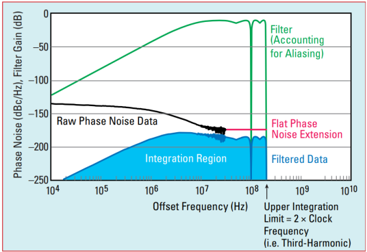
Fig. 6 Summary of the recommended phase noise methodology for a 100 MHz clock, which appends
a flat phasenoise extension up to 2× the clock frequency, before filtering and integrating to derive jitter. 3
CONCLUSION
The clock and timing industry typically derive jitter in clock signals from phase noise analyzer measurements. On the other hand, high-speed serial-data communications standards typically measure jitter in serial-data signals using an oscilloscope.
Recent increases in data rates require lower-jitter reference clocks, to the point where today, jitter added by an oscilloscope-based test environment can no longer be ignored. This motivated creating a methodology based on phase noise that yields the same jitter values obtained from a traditional oscilloscope methodology.
The phase noise methodology provides the best match to oscilloscope-based jitter results is summarized.1 The methodology accounts for aliasing of phase noise in sampled systems (e.g. PLLs) by extending the last-measured data point up to an offset frequency equal to twice the fundamental clock frequency. We postulate this methodology providing the best match to oscilloscope-based jitter results because the phase noise at the third harmonic dominates the integral when computing jitter, beyond which the phase noise spectrum rolls off to insignificant levels.
This phase noise methodology was adopted into PCI Express Base Specification Revision 5.0 Version 1.011 as an alternative normative test to the traditional PCI-SIG oscilloscope-based refclk jitter methodology.
In summary, the phase noise methodology presented here is much faster and simpler to implement than the corresponding oscilloscope methodology. Since a phase noise analyzer has a lower noise floor than an oscilloscope, this methodology also scales more easily as timing margins shrink in future high-speed serial links. Finally, this methodology is a more natural fit for analyzing clock signals than an oscilloscope methodology, since phase noise data is readily available for precision clock sources.
Note: PCI, PCI Express, PCIe, and PCI-SIG are trademarks or registered trademarks of PCI-SIG. All opinion, judgments, and recommendations presented herein are the opinions of the author and do not necessarily reflect on the opinions of the PCI-SIG®.
REFERENCES
1. G. Giust, “Methodology for Analyzing Reference-Clock Phase Noise in HighSpeed Serial Links,” Signal Integrity Journal, May 3, 2019, www.signalintegrityjournal.com/articles/1216.
2. G. Giust, “Phase Noise Aliases as TIE Jitter,” Signal Integrity Journal, July 23, 2018, hwww.signalintegrityjournal.com/articles/912.
3. “Method and Apparatus for Analyzing Phase Noise in a Signal From an Electronic Device,” Patent Pending, JitterLabs LLC.
4. G. Giust, “Influence of Noise Processes on Jitter and Phase Noise Measurements,” Signal Integrity Journal, April 8, 2018, www.signalintegrityjournal.com/ articles/800.
5. “PCI Express Base Specification Revision 4.0 Version 1.0,” PCI-SIG, September 27, 2017, www.pcisig.com.
6. “PCI Express Base Specification Revision 5.0 Version 1.0,” PCI-SIG, Draft April 25, 2019, www.pcisig.com.
7. G. Richmond, “Refclk Fanout Best Practices for 8GT/s and 16GT/s Systems,” PCI-SIG Developers Conference, June 7, 2017.
8. G. Giust, “Methodologies for PCIe5 Refclk Jitter Analysis,” PCI-SIG Electrical Workgroup Meeting, January 19, 2018.
9. G. Giust, “Study to Determine a Phase Noise Methodology that Matches Jitter Measurements from a Scope,” PCI-SIG Electrical Workgroup Meeting, May 24, 2018.
10. “Determine the Dominant Source of Phase Noise, by Inspection,” G. Giust, Note4, JitterLabs LLC, www.jitterlabs.com/support/publications/note4/note4.
11. “PCI Express Base Specification Revision 5.0 Version 0.9, Section 8.6.7,” PCISIG, October 18, 2018, www.pcisig.com.