Glossary of Oscillator Terminology
Part 1. Types of Timing Devices
Crystal (X or XTAL)
Crystal Oscillator (XO) or Oscillator
Digitally Controlled Crystal Oscillator (DCXO) or Digitally Controlled Oscillator
Digitally Controlled Temperature Compensated Crystal Oscillator (DCTCXO)
Oven-Controlled Crystal Oscillator (OCXO)
Temperature Compensated Crystal Oscillator (TCXO) or Temperature Compensated Oscillator
Voltage Controlled Crystal Oscillator (VCXO)
Voltage Controlled Oscillator Voltage Controlled Temperature Compensated Crystal Oscillator (VCTCXO)
Part 2. Oscillator Terminology
Absolute Pull Range (see Pull Range)
Activity Dip
Aging
Allan Deviation
Clipped Sinewave Output
CML
Cycle to Cycle Jitter
DPPM
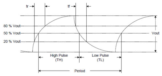
Duty Cycle
Frequency
Frequency vs Temperature Slope
Frequency Stability
Gain Transfer or Kvco
Hadamard Variance
HCSL
Holdover
Integrated Phase Jitter (IPJ)
Load
Long-Term Jitter
LVCMOS
LVDS
LVPECL
MEMS
MTBF
Operating Temperature Range
Output Enable
Packaging
Parts per Million (ppm) and Parts per Billion (ppb)
Period Jitter
Phase Noise
Pullability
Pull Linearity
Pull Range – Total Pull Range and Absolute Pull Range
Quality Factor, Q
Retrace
Rise/Fall Time
Single-Ended SPL
Standby
Start-up Time
Supply Current
Supply Voltage
Total Pull Range (see Pull Range)
Thermal Hysteresis
Tri-State
VOH/VOL
1. Types of Timing Devices
Crystal (X or XTAL)
A crystal is a passive resonator that vibrates at a fixed frequency. Crystals are used as an external timing reference for semiconductor ICs with an integrated oscillator circuit (i.e., on-chip generation).
Crystal Oscillator (XO) or Oscillator
An oscillator is an active device that combines the resonator and oscillator circuit into a single package. Oscillators do not require external components to generate a clock signal. Although in some cases, power supply decoupling components and/or termination resistor(s) may be required. In some regions, XOs are referred to as OSC or SPXO (simple packaged crystal oscillator). Typical frequency stability of XOs ranges from ±10 to ±100 ppm.
The minimum pin count for single-ended oscillators is three pins for power, ground, and the oscillator output. However oscillators usually have at least four pins to accommodate output enable or other control functions. Differential oscillators are usually packaged in six-pin packages. Some oscillators which include serial interface control such as I2 C are packaged in 10-pin or higher pin-count packages. Frequency stability for XOs usually ranges from ±10 ppm to ±100 ppm and they are usually offered in the following packages: 7050, 5032, 3225, 2520, and 2016.
Digitally Controlled Crystal Oscillator (DCXO) or Digitally Controlled Oscillator
A DCXO is similar to a VCXO in that both types of devices allow pulling the frequency. In some cases, DCXOs have the capability to program output frequency to a wider range beyond the limited pull range. The difference with DCXOs compared to VCXOs, is that frequency is adjusted by writing digital control words over a serial interface such as I2 C or SPI.
Digitally Controlled Temperature Compensated Crystal Oscillator (DCTCXO) or Digitally Controlled Temperature Compensated Oscillator
A DCTCXO is a TCXO that incorporates the frequency pulling and programming functionality of a DCXO.
Oven Controlled Crystal Oscillator (OCXO)
An OCXO provides temperature compensation and ovenization to maintain an almost constant temperature for the oscillator at as ambient temperature varies. These devices enclose the resonator, along with temperature-sensing and compensation circuits inside a heated enclosure. This temperature compensation and ovenization enables the OCXO to achieve very good frequency stability ranging from 0.05 ppb to 200 ppb. The typical package size of a quartz-crystal OCXO ranges from to 9.7 mm x 7.5 mm to 135 mm x 72 mm.
Temperature Compensated Crystal Oscillator (TCXO) or Temperature Compensated Oscillator
A TCXO is an oscillator that incorporates temperature compensation to compensate for the frequency vs. temperature characteristic of the resonator. This compensation enables TCXOs to achieve better frequency stability than non-compensated oscillators (XOs). Frequency stability of TCXOs ranges from ±0.05 ppm to ±5 ppm. These devices are used in applications where precision timing references are required such as high performance telecom and networking equipment.
Voltage Controlled Crystal Oscillator (VCXO) or Voltage Controlled Oscillator
VCXOs incorporate a control voltage pin that controls the output frequency around the nominal frequency. The extent of frequency control is called the pull range which typically ranges from ±50 ppm to ±200 ppm but can extend to ±3200 ppm for SiTime VCXOs. VCXOs are often used in discrete jitter attenuation and clock recovery applications.
Voltage Controlled Temperature Compensated Crystal Oscillator (VCTCXO) or Voltage Controlled Temperature Compensated Oscillator
A VCTCXO is a TCXO that incorporates a control voltage pin to allow the output frequency to vary around the nominal frequency. The frequency tuning range for a VCTCXO is typically ±5 ppm to ±25 ppm. Some vendors refer to these devices as TCVCXOs.
Note regarding SiTime MEMS-based oscillators
While all of SiTime’s devices use MEMS resonators and not quartz crystal resonators, SiTime does not replace the “X” in the above acronyms with “M” (for MEMS) because these product categories and acronyms have been established in the industry for decades and are associated with certain timing functions. As SiTime devices offer the same or better functionality as quart-based products, it causes less confusion to continue with the same well-known product classifications and acronyms.
2. Oscillators Terminology
Absolute Pull Range
See Pull Range
Activity Dip
Activity dips result from mechanical coupling of the principal resonance mode to one or more interfering modes that exist but are not electrically excited by the sustaining circuit. Resonance frequencies of these modes shift as the environmental temperature changes. At some temperatures, the frequency of the interfering mode(s) may come close to the frequency of the desired mode, causing the main mode to loose energy. This, in turn, causes an increase in the resonator equivalent resistance which manifests as a shift in output frequency.
This shift is usually a rapid jump in the frequency over temperature characteristic. After the frequency jumps, the smooth frequency curve continues on a similar trajectory as before, but it is shifted up or down due to the jump. This rapid frequency change can cause system problems such as PLL unlock or packet loss. Quartz-based resonators are susceptible to activity dips. However, SiTime MEMS-based resonators are free of activity dips.
Aging
Aging is the change in oscillator frequency, measured in ppm over a certain time period, typically reported in months or years. This change in frequency with time is due to internal changes within the oscillator, while external environmental factors are kept constant.
Note regarding SiTime MEMS-based oscillators
SiTime MEMS oscillators aging data is provided for up to a 10-year period. SiTime oscillator aging is significantly lower (better) than quartz oscillators because MEMS resonators are vacuum sealed in silicon using a process that eliminates foreign particles that can affect aging.
Allan Deviation
Also known as short-term frequency stability, Allan deviation (ADEV) is the measure of oscillator stability in the time-domain. It represents a frequency change over an interval of time called averaging time. Allan deviation is calculated as the root mean square (RMS) change in successive frequency measurements. The averaging time typically ranges from milliseconds to thousands of seconds depending on the target application. The formula for Allan deviation is shown below, where the y values represent the values of fractional frequency deviation between adjacent clock cycles and M is the sample size.
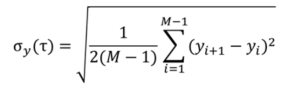
Allan deviation is used for clock oscillators because it converges for more types of oscillator noise compared to standard deviation. Allan deviation converges for white phase modulation, flicker phase modulation, white frequency modulation, flicker frequency modulation, and random walk frequency. Allan deviation does NOT converge for flicker walk frequency modulation and random run frequency modulation.
Clipped Sinewave Output
Clipped sinewave is a common single-ended output format often encountered in TCXO (temperature controlled oscillator) or OCXO (oven controlled oscillator) devices. The main feature of clipped sinewave output is very slow gradual rising and falling edges that resemble portions of the sinewave, hence the name. Slow rise/fall times have several benefits including reduced energy of high-frequency output harmonics that are undesirable in RF applications. This helps achieve good signal integrity with fewer restrictions in the layout rules. The drawback is slightly lower jitter performance at high frequencies compared to LVCMOS output.
The diagram below shows a typical clipped sine waveform and the significantly slower rise and fall times.
CML
Current mode logic (CML) is a common oscillator differential output format. It is an open drain type output which means the driver only drives low and that external pull-up resistors are required to pull the clock signal high during the high portion of the clock period. Two voltage swings are commonly supported, 450 mV and 850 mV. The diagram below shows a typical 450 mV waveform. CML is commonly used in telecom infrastructure applications such as wireless base stations.
Cycle to Cycle Jitter
Cycle to cycle (C2C) jitter is defined as the variation in cycle time of a signal between adjacent cycles. It is measured over a random sample of adjacent cycle pairs (JEDEC JESD65B). The suggested minimum sample size is 1,000 cycles as specified by JEDEC.
See related terms: Integrated Phase Jitter (IPJ), Long-Term Jitter, Period Jitter, Phase Noise
Differential
In contrast to single-ended output, differential output consists of two complementary signals with 180° phase difference between the two signals. This output type is often used in high-frequency oscillators (100 MHz and above). Differential signals usually have lower voltage swing than single-ended signals, faster rise/fall times, better noise immunity, and are used when better performance or higher frequency is required. The most commonly used differential signally types are LVPECL, LVDS, and HCSL.
See related term: Single-Ended
DPPM
DPPM (defective parts per million) quantifies how many units may be defective per 1 million units. This unit of measurement is estimated with certain degree of confidence.
Duty Cycle
Duty cycle is a clock signal specification that is defined as the ratio in percentage between the pulse duration in high state to the period of the oscillator signal. The diagram below illustrates duty cycle % = 100* TH/Period, where TH and Period are measured at the 50% point on the waveform. Typical duty cycle specifications range from 45% to 55%.
Frequency
Frequency is the repetition rate (cycle) of the signal output from the oscillator and is measured in Hertz (Hz) per second. Many applications call for a specific oscillator frequency. Following is a list of standard frequencies and their typical applications.
Output Frequency (MHz) Application
0.002000 Frame Clock
0.008000 BITS Clock
0.032768 Real Time Clock
1.544000 Telecom DS1
2.048000 Telecom E1
8.000000 Automotive CAN Bus
8.192000 ISDN
9.830400 Wireless CMA, UART
10.000000 GPS Disciplined Oscillator, Network Time Protocol, test and Measurement
12.000000 USB/Automotive CAN Bus
12.288000 DAT Digital Audio
12.352000 Telecom DS1
12.800000 Common OCXO Frequency for Telecom
13.500000 Audio/Video
14.318180 NTSC Clock, Crystal Reference for PC Motherboard clock
19.200000 GSM/UMTS
24.576000 Audio, IEEE1394
25.000000 Ethernet
26.000000 GSM/UMTS
26.562500 Fibre Channel
27.000000 Audio/Video
32.000000 Wireless IoT
30.720000 Wireless W-CDMA
33.33333313 Parallel PCI
34.368000 Telecom E3
38.880000 Telecom SONET
40.000000 WIFI, SCSI, CPU Reference
44.736000 DS3
48.000000 USB
50.000000 Ethernet, General Purpose
53.125000 Fibre Channel
61.440000 W-CDMA
66.66666625 Parallel PCI, PCI-X General Purpose
74.17582418 Video
74.250000 Video
75.000000 SATA
77.760000 SONET
96.000000 USB
100.000000 PCI Express/General Purpose
106.250000 Fibre Channel
122.880000 W-CDMA
125.000000 1G Ethernet
133.3333325 PCI-X, General Purpose
148.3516484 Video
148.500000 Video
150.000000 SATA
153.600000 W-CDMA
155.520000 SONET
156.250000 10G Ethernet
159.375000 Fibre Channel
161.1328125 10G Ethernet (156.25 * 66/64 Line Coding)
166.6666656 Computing
168.040678 OTU3 (155.52 * 235/236 FEC)
175.000000 General Purpose
187.500000 Ethernet
200.000000 General Purpose
212.500000 Fibre Channel
233.3333333 Computing
250.000000 SAN/General Purpose
266.666665 Computing
300.000000 SATA/General Purpose
311.040000 SONET
312.500000 Ethernet
322.265625 Ethernet (312.5 * 66/64 Line Coding)
333.3333331 Computing
350.000000 General Purpose
425.000000 Fibre Channel
614.400000 W-CDMA
625.000000 Ethernet
637.500000 Fibre Channel
644.531250 OTU3 (625 * 66/64 Line Coding), 100GbE, 400 GbE
700.000000 General Purpose
1250.000000 Ethernet
1275.000000 Fibre Channel
Note regarding SiTime MEMS-based oscillators
SiTime oscillators are available in frequencies as low as 1 Hz for low-power devices and as high as 725 MHz. The frequency of SiTime oscillators is programmable within this range to 6 decimals of accuracy. Frequency can be factory programmed by SiTime, programmed by key partners and distributors, or programmed for lower volumes in the customer’s lab using an oscillator programmer.
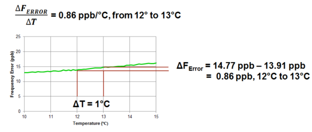
Frequency vs Temperature Slope
Frequency vs temperature slope, also shown as ΔF/ΔT, is the rate of frequency change due to a 1°C change in temperature. It quantifies sensitivity of the oscillator frequency to small temperature variations near the operating temperature point. It is one of the major performance metrics of precision TCXOs that determines if the TCXO is stable enough to support the needs of the target application. Smaller frequency vs temperature slope values mean lower frequency variation due to the temperature change in a confined temperature window. For example, an average system temperature window may be ±5°C.
In systems that require time and frequency transfer using IEEE 1588, better frequency vs temperature slope helps improve time error. The unit of measure is in ppm/°C or ppb/°C. Below is a plot of the SiT5356 Elite TCXO showing the frequency slope from 12°C to 13°C with a value of 0.86 pb/°C. This plot shows frequency error vs. the nominal frequency instead of absolute frequency, hence the y-axis label FERROR. The frequency vs. temperature slope is reported as the highest absolute value of slopes observed over the total temperature range.
Frequency Stability
Frequency stability is a fundamental performance specification for oscillators. This specification represents the deviation of output frequency due to external conditions – a smaller stability number means better performance. The definition of external conditions can differ for different oscillator categories, but usually includes temperature variation. It may also include supply voltage variation, output load variation, and frequency aging. Frequency stability is typically expressed in parts per million (ppm) or parts per billion (ppb) which is referenced to the nominal output frequency.
Gain Transfer or Kvco
Gain transfer or Kvco is a common characteristic of voltage controlled oscillators (VCXOs) that determines how much output frequency changes in response to a 1-V change in control voltage. This is useful in calculating the characteristics of closed loops that utilize a VCXO.
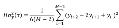
Hadamard Variance
Hadamard variance is the square of the change in three successive frequency measurements. These measurements are the values of fractional frequency deviation between three adjacent clock cycles and M is the sample size. Hadamard variance converges for white phase modulation, flicker phase modulation, white frequency modulation, flicker frequency modulation, random walk frequency, flicker walk frequency modulation and random run frequency modulation. It is unaffected by linear frequency drift and well suited for analysis of Rubidium oscillators. Below is the formula for Hadamard variance, where y represent the values of fractional frequency deviation among three contiguous clock cycles and M is the sample size.
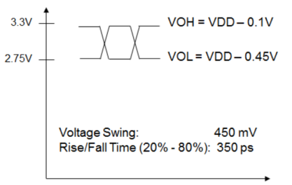
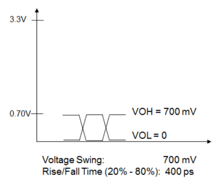
HCSL
High speed current steering logic (HCSL) is a commonly used differential output format used for PCI Express, servers, and other applications. As shown below, it has a typical output swing of 700 mV and swings from 0V to 700 mV.
See related terms: LVDS, LVPECL
Holdover
Holdover is a mode of operation used by systems that are synchronized to an external precision frequency and/or time reference, and that have temporarily lost this reference signal. The local oscillator should have the capability to maintain, or holdover, stable frequency and/or time within the defined limits in a system after the loss of the external reference.
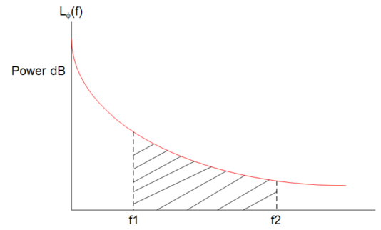
Integrated Phase Jitter (IPJ)
Phase jitter is the integration of phase noise over a certain spectrum and is expressed in picoseconds or femtoseconds. The diagram below shows an example integration band between f1 and f2 and the area under this curve is time domain picoseconds or femtoseconds of jitter.
See related terms: Cycle to cycle (C2C) jitter, Long-Term Jitter, Period Jitter, Phase Noise
Load
Within the scope of oscillators, load usually refers to capacitive load – the total capacitance driven by the oscillator output. Load consists of the input capacitance of the driven IC, trace capacitance, plus any other parasitics or passive components on the printed circuit board.
Long-Term Jitter
Long-term jitter measures the deviation of clock features from the ideal position over several consecutive clock cycles. This effectively measures how the duration of a number of consecutive clock cycles deviates from its mean value.
See related terms: Cycle to cycle (C2C) jitter, Integrated Phase Jitter (IPJ), Period Jitter, Phase Noise
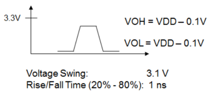
LVCMOS
Low voltage CMOS (LVCMOS) is the most common single-ended output interface standard used by oscillators. Low voltage usually means less than 5V and includes 3.3V, 2.5V, 1.8V, and lower voltages. The output swing is ideally rail to rail (0V to VDD) but is typically not quite full rail at the receiver due to losses. The diagram below shows an example of a 3.3V LVCMOS signal.
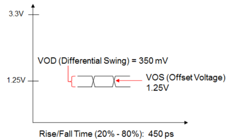
LVDS
Low voltage differential (LVDS) signaling is a common oscillator differential output format. It is usually lower power than other differential outputs and has a voltage swing of about 350 mV. This output format is commonly used in network switches, routers, wireless base stations, and telecom transmission systems. Below is a typical LVDS output waveform.
See related terms: HCSL, LVPECL
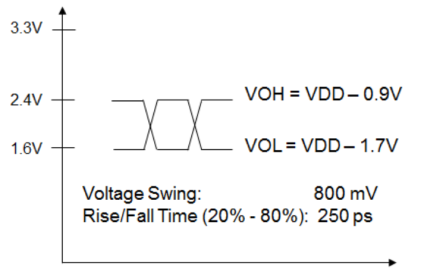
LVPECL
Low voltage positive emitter-coupled logic (LVPECL) is a common oscillator differential output format. It has a voltage swing of about 800 mV with the differential cross point at around 2V. LVPECL is used in applications where low noise is important such as network switches, routers, wireless base stations, and telecom transmission systems. The key features of LVPECL are the constant current source driver and the fact the transistors never go into saturation, which are key to low noise and fast switching speed respectively. The diagram below shows a typical differential LVPECL waveform.
See related terms: HCSL, LVDS
MEMS
Micro-electro-mechanical systems (MEMS) is the technology of microscopic devices with moving parts. In some regions, this technology is known as micro-machines or micro-systems technology. MEMS evolved from process technologies used in the fabrication of semiconductor devices. Therefore, silicon is the most common material used for manufacturing MEMS components.
MEMS technology is used a wide variety of commercial applications including accelerometers, gyroscopes, microphones, and a range of sensors. MEMS have been commercially used as an alternative to quartz crystal resonators and shipping in production volume since in 2007.
For more information see SiTime's MEMS First™ and EpiSeal™ Processes Technology Paper.
MTBF
Mean time between failures (MTBF) is the predicted time between oscillator failures. Quartz-based devices usually have a MTBF in tens of millions of hours. SiTime oscillators have a MTBF of over 1 billion hours. Another measure of quality is failure in time (FIT) rate which is a number of failures in a unit of time such as millions of hours or billions of hours.
For more information see SiTime Reliability Calculations Application Note.
Operating Temperature Range
Operating temperature range is the temperature span in which all oscillator parameters are specified within in the datasheet. Common temperature ranges are listed below.
Commercial, Automotive Grade 4: 0°C to 70°C
Extended Commercial: -20°C to 70°C
Industrial, Automotive Grade 3: -40°C to 85°C
Extended Industrial, Automotive Grade 2: -40°C to 105°C
Automotive Grade 1: -40°C to 125°C
Military: -55°C to 125°C
Automotive Grade 0: -40°C to 150°C
Output Enable
Output enable (OE) is a feature that is used to control the oscillator output state via a digital input signal. The output enable function means that the device outputs the frequency when the control pin is pulled high and it is disabled when the pin is pulled low.
Packaging
2016: 2.0 x 1.6 mm
2520: 2.5 x 2.0 mm
3225: 3.2 x 2.5 mm
5032: 5.0 x 3.2 mm
7050: 7.0 x 5.0 mm
OCXOs are housed in significantly larger packages that range from 9.7 x 7.5 mm to 135 x 72 mm. A common OCXO package size is 25.4 x 25.4 mm.
Note regarding SiTime MEMS-based oscillators
In addition to these standard package sizes, SiTime offers kHz and MHz oscillators in a 1.54 x 0.84 mm chip-scale package, which is the smallest oscillator package available.
Parts per Million (ppm) and Parts per Billion (ppb)
These are relative units of frequency with respect to the nominal frequency. 1 ppm means 1/106 part of a nominal frequency. 1 ppb means 1/109 part of a nominal frequency.
Period Jitter
Period jitter is the deviation in cycle time of a clock signal over a number of randomly selected cycles (JEDEC JESD65B). The suggested minimum sample size is 10,000 cycles. The process for obtaining and computing period jitter is as follows.
- Measure the duration (rising edge to rising edge) of one clock cycle
- Wait a random number of clock cycles
- Repeat the above steps 10,000 times
- Compute the mean, standard deviation (σ), and the peak-to-peak values from the 10,000 samples.
See related terms: Cycle to cycle (C2C) jitter, Integrated Phase Jitter (IPJ), Long-Term Jitter, Phase Noise
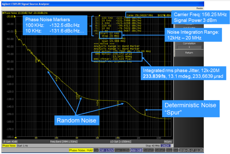
Phase Noise
In an oscillator, phase noise is the rapid, short-term, random fluctuation of the phase of a clock signal, caused by time-domain instabilities. Phase noise L[f] is expressed in decibels relative to carrier power (dBc) per 1-Hz bandwidth. It is related to the spectral density of phase fluctuations S(f) as L[f] = 10log[0.5S(f)] (US Federal Standard 1037°C, Glossary of Telecommunication Terms). In simpler terms, phase noise is a frequency domain measure of what manifests as clock jitter in the time domain. Following is a phase noise plot of a SiTime SiT9365 oscillator that highlights key information related to phase noise.
See related terms: Cycle to cycle (C2C) jitter, Integrated Phase Jitter (IPJ), Long-Term Jitter, Period Jitter
Pullability
Pullability is the ability to control or pull oscillator output frequency over a narrow range from the nominal frequency value. The typical means of frequency control is a control voltage applied to the control voltage input pin for VCXOs. DCXOs (digitally controlled crystal oscillators) allow pulling the frequency by writing digital control words over a serial interface such as I2 C or SPI. Pullability range varies in oscillators from ±5 ppm to ±3200 ppm.
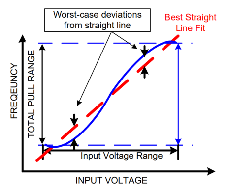
Pull Linearity
Pull linearity is one of the characteristics that determine the quality of a VCXO. The response of the VCXO frequency to control voltage change over the full pull range should ideally be a straight line. Pull linearity quantifies how far the real characteristic is away from the perfect line. It is defined as the ratio between frequency error from the expected value to the total deviation, expressed in percent, where frequency error is the maximum frequency excursion from the so-called “Best Straight Line” drawn through a plot of output frequency vs control voltage. The diagram below illustrates this concept.
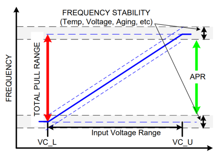
Pull Range – Total Pull Range and Absolute Pull Range
Total pull range (PR) is the amount of frequency deviation that results from changing the control voltage over its maximum range under nominal conditions. Absolute pull range (APR) is the guaranteed controllable frequency pull range of a voltage controlled oscillator over all environmental and aging conditions. The diagram below shows the relationship between pull range and absolute pull range.
Quality Factor, Q
Quality factor is proportional to the ratio of energy stored to energy dissipated per cycle of an oscillator as shown in the equation below.
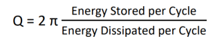
Higher Q represents a better, more underdamped oscillator because less energy is lost per cycle. Q impacts close to carrier phase noise with higher Q resulting in lower (better) phase noise. The Q of an AT cut quartz resonator ranges from 10,000 to 100,000. SiTime MEMS resonators have a typical Q of 150,000.
Note regarding quartz vs SiTime MEMS resonators
The Q of an AT cut quartz resonator ranges from 10,000 to 100,000. SiTime MEMS resonators have a typical Q of 150,000.
Retrace
Retrace is the frequency error between multiple consecutive power cycles of the oscillator. It shows how well the oscillator returns to the same absolute frequency after the power has been removed for some time and applied back to the device. Retrace is of particular importance in precision oscillators such as OCXOs.
The causes of retrace are not fully understood, but can involve strain changes in the resonator’s mounting structure and contamination redistribution inside the package. SiTime TCXOs have among the industry’s lowest (best) retrace, typically less than ±10 ppb, because of extremely low contamination levels on the order of parts-per-billion (ppb) due to wafer-level encapsulation of the resonator.
Note regarding SiTime MEMS-based oscillators
SiTime TCXOs have among the industry’s lowest (best) retrace, typically less than ±10 ppb, because of extremely low contamination levels on the order of parts-per-billion (ppb) due to wafer-level encapsulation of the resonator.
Rise/Fall Time
Rise/fall time is the duration of the rising and falling edge of the output signal typically measured between 20% and 80% or 10% and 90% of the output signal levels. The diagram below shows rise and fall time defined for 10% to 90% on a single-ended output.
Single-Ended
In contrast to differential output, single-ended output consists of a single output clock, usually LVCMOS, which swings approximately rail to rail (0V to VDD). Single-ended output is the most common oscillator output type.
SPL
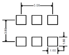
Solder pad layout (SPL) is the layout of the printed circuit board landing pads upon which the oscillator sits. The example below shows an SPL for a 6-pin 7050 oscillator package (7.0 mm x 5.0 mm).
Standby
Standby is a low-power mode where most of the internal circuitry is completely shut down and the oscillator does not produce any output frequency. Initiated setting digital control input pin into appropriate state.
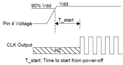
Start-up Time
Start-up time is the time period from when supply voltage (VDD) is applied (90%) to the oscillator and when the first output clock cycle begins. The diagram below illustrates start-up time.
Supply Current
Supply current is the maximum operating current of an oscillator. It is measured in microamps (µA) or milliamps (mA) at the maximum and sometimes nominal supply voltage. Typical supply current is measured without load.
Supply Voltage
Supply voltage, specified in volts (V), is the input power required to operate the oscillator. Supply voltage powers the oscillator through the VDD pin and is sometimes referred to as VDD. Standard voltages for single-ended oscillators include 1.8, 2.5, and 3.3V. Voltages for modern differential oscillators typically range between 2.5 and 3.3V. SiTime offers oscillators that operate as low as 1.2V for regulated supply applications such as coin-cell or super-cap battery backup. The supply voltage of most SiTime oscillator families is programmable, which reduces the need for external components such as level translators or voltage regulators.
Note regarding SiTime MEMS-based oscillators
SiTime offers oscillators that operate as low as 1.2V for regulated supply applications such as coincell or super-cap battery backup. The supply voltage of most SiTime oscillator families is programmable, which reduces the need for external components such as level translators or voltage regulators. Voltage can be factory programmed by SiTime, programmed by key distributors, or programmed for lower volumes in the customer’s lab using an oscillator programmer.
Thermal Hysteresis
Thermal hysteresis is the difference between up-cycle and down-cycle frequency over temperature characteristics and is quantified by the value of the difference at the temperature where the difference is at its maximum. Thermal hysteresis is especially important for precision oscillators such as TCXOs and OCXOs because it consumes a significant portion of the overall frequency stability budget.
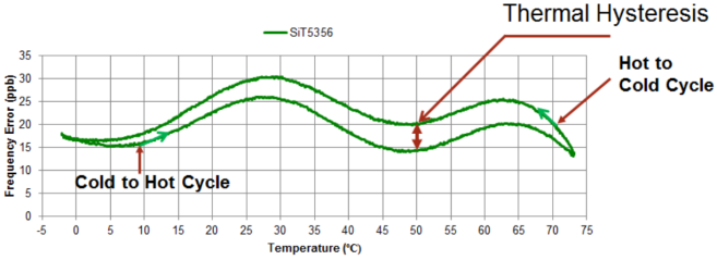
The causes of thermal hysteresis are not fully understood, but can involve strain changes in the resonator mounting structure, contamination redistribution inside the package, and a thermal gradient between the temperature sensor and resonator. SiTime TCXOs have among the industry’s lowest (best) hysteresis, typically ±15 ppb over -40°C to 105°C, because of the negligible thermal lag between the oscillator and temperature sensor and the extremely low contamination levels on the order of parts-perbillion (ppb) due to wafer level encapsulation of the resonator.
Total Pull Range
See Pull Range
Tri-State
Tri-state is the high impedance output state that typically occurs when the output is shut down by disabling the output driver and no clock signal is produced.
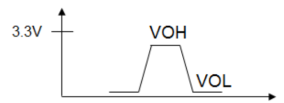
VOH/VOL
Voltage output high/voltage output low (VOH/VOL) are the high and low voltage levels of the clock output. The diagram below shows how VOH and VOL relate to the clock waveform.