SiT6502EB Evaluation Board (EVB) HW User Manual
Content
1. Introduction
2. SiT6502EB Features
3. SiT6502EB Support Collateral
4. Connectors Descriptions
5. Test Points Descriptions
6. Jumpers Default List
7. Default Resistor Connection from FTDI to SiT95147
8. Status LEDs
9. SiT6502EB Power Supplying
10. I2C/SPI Mode Connection
11. Clock Inputs
12. Clock Outputs
12.1 Output Differential Termination
12.1.1 LVDS, CML
12.1.2 LVPECL
12.1.3 HCSL
13. Quick Start
Appendix A: EVB Schematic Diagrams
Appendix B: EVB Top View
1. Introduction
The SiT6502EB evaluation board (EVB) is designed for evaluating the programmable SiT95147 jitter cleaner/attenuator.
2. SiT6502EB Features
- Powered from USB port or external power supply
- Programmable VDDO supplies for each of the 8 outputs selectable from 3.3, 2.5, or 1.8 V
- Status LEDs for power supplies status signals of SiT6502EB - Each of the 8 outputs accessible via edge mount
- High bandwidth SMA connectors
- 4 pairs of edge mount SMA connectors for feeding external differential or single-ended clocks
- Supports full configuration flexibility of the device via standard I2C or SPI interface with a Windows-hosted Time Master for Clocks GUI
3. SiT6502EB Support Collateral
The SiT6502EB Evaluation Board is provided with the following collateral:
- SiT6502EB EVB HW User Manual
- Time Master for Clocks SW
- Time Master for Clocks SW User Manual
4. Connectors Descriptions
Table 1 lists the SiT6502EB EVB connectors:
| Connector Designators | Description |
|---|---|
| Power + Control | USB Type B connectors (J3) for Device programming and +5V supply |
| Power | USB Type B connectors (J4) for +5V supply, 2-pin connectors (J80, J7) for external +5V power supply |
| Inputs | SMA connectors (J35 through J42) for receiving external clock signals |
| Outputs | SMA connectors (J43 through J62) for synthesized clock outputs |
| External FTDI supply | 2-pin connector (H13) |
| External +3.3V (VDD Left) Input receiver supply | 2-pin connector (H1) |
| External +3.3V (VDD PLL) supply | 2-pin connector (H12) |
| External Output VDD Supply | 2-pin connectors (H2 through H11) |
| Common Mode to GND Headers in output terminations | 2-pin Headers (JSCL13 through JSCL22) |
| Output LDO Regulators Enable Inputs to GND Headers | 2-pin Headers (J2, JSCL3 through JSCL11), shorted by default for LDO outputs enabling |
| Left Supply LDO Regulators Enable Inputs to GND Headers | 2-pin Headers (J1), shorted by default for LDO outputs enabling |
| Header for internal use only | 2-pin Header (JSCL 1), shorted by default |
| Headers for I2C bus Pull-up | 2-pin Headers (JSCL 2, JSCL 12), shorted by default |
| Header | 1-pin Header (J5) |
| Header for PLL supply LDO regulator output Shut Down | 2-pin Header (J12) |
| Header for internal use only | 10-pin Header (J76) (Default Jumper position see in Figure A20) |
| PullUp vs PullDown switch Headers | 3-pin Headers (J67 through J69, J72 through J74, J75, J81, JVDD1) |
| Signals switch Header | 3-pin Header (J71) |
| PLL supply voltage source switching Header | 3-pin Header (J31) |
| PLL supply voltage levels switching Header | 3-pin Header (J32) |
| Left supply voltage source switching Header | 3-pin Header (J8) |
| Left supply voltage levels switching Header | 3-pin Header (J9) |
| FTDI supply voltages source switching Header | 3-pin Header (J78) |
| FTDI supply voltage levels switching Header | 3-pin Header (J30) |
| USB – External Power sources switching Headers | 3-pin Headers (J79, J6) |
| Outputs supply voltage source switching Header | 3-pin Headers (J10, J77, J14, J16, J18, J20, J22, J24, J26, J28) |
| Outputs supply voltage levels switching Header | 3-pin Headers (J11, J13, J15, J17, J19, J21, J23, J25, J27, J29) |
5. Test Points Descriptions
Table 2 describes all Test Point (TP)s on the EVB:
| Connector Designators | Description |
|---|---|
| GND Test Points | 1-pin Headers (TP1, TP3, TP4, TP5, TP7) |
| Reference Clock Test Point | 1-pin Header (TP6) |
| Test Points for internal use only | 1-pin Headers (TP2, TP8, J82 through J86) |
6. Jumpers Default List
Table 3 lists the default positions of the Jumpers on the EVB:
| Jumper Location | Type | I = Installed O = Open |
Jumper Location | Type | I = Installed O = Open |
Jumper Location | Type | I = Installed O = Open |
|---|---|---|---|---|---|---|---|---|
| JSCL1 | 2-Pin | I | J1 | 2-Pin | I | J28 | 3-Pin | 1 to 2 |
| JSCL2 | 2-Pin | I | J2 | 3-Pin | 1 to 2 | J29 | 3-Pin | 1 to 2 |
| JSCL3 | 2-Pin | I | J6 | 3-Pin | 2 to 3 | J30 | 3-Pin | 1 to 2 |
| JSCL4 | 2-Pin | I | J8 | 3-Pin | 1 to 2 | J31 | 3-Pin | 1 to 2 |
| JSCL5 | 2-Pin | I | J9 | 3-Pin | 1 to 2 | J32 | 3-Pin | 2 to 3 |
| JSCL6 | 2-Pin | I | J10 | 3-Pin | 1 to 2 | J67 | 3-Pin | O |
| JSCL7 | 2-Pin | I | J11 | 3-Pin | 1 to 2 | J68 | 3-Pin | O |
| JSCL8 | 2-Pin | I | J12 | 2-Pin | O | J69 | 3-Pin | O |
| JSCL9 | 2-Pin | I | J13 | 3-Pin | 1 to 2 | J71 | 3-Pin | O |
| JSCL10 | 2-Pin | I | J14 | 3-Pin | 1 to 2 | J72 | 3-Pin | O |
| JSCL11 | 2-Pin | I | J15 | 3-Pin | 1 to 2 | J73 | 3-Pin | 1 to 2 |
| JSCL12 | 2-Pin | I | J16 | 3-Pin | 1 to 2 | J74 | 3-Pin | O |
| JSCL13 | 2-Pin | O | J17 | 3-Pin | 1 to 2 | J75 | 3-Pin | 2 to 3 |
| JSCL14 | 2-Pin | O | J18 | 3-Pin | 1 to 2 | J76 | 10-Pin Header | 1 to 2, 3 to 4, 7 to 8, 9 to 10 |
| JSCL15 | 2-Pin | O | J19 | 3-Pin | 1 to 2 | J77 | 3-Pin | 1 to 2 |
| JSCL16 | 2-Pin | O | J20 | 3-Pin | 1 to 2 | J78 | 3-Pin | 1 to 2 |
| JSCL17 | 2-Pin | O | J21 | 3-Pin | 1 to 2 | J79 | 3-Pin | 1 to 2 |
| JSCL18 | 2-Pin | O | J22 | 3-Pin | 1 to 2 | J80 | 2-Pin | O |
| JSCL19 | 2-Pin | O | J23 | 3-Pin | 1 to 2 | J81 | 3-Pin | O |
| JSCL20 | 2-Pin | O | J24 | 3-Pin | 1 to 2 | J87 | 3-Pin | O |
| JSCL21 | 2-Pin | O | J25 | 3-Pin | 1 to 2 | J88 | 3-Pin | O |
| JSCL22 | 2-Pin | O | J26 | 3-Pin | 1 to 2 | J89 | 3-Pin | O |
| JVDD1 | 3-Pin | 2 to 3 | J27 | 3-Pin | 1 to 2 |
7. Default Resistor Connection from FTDI to SiT95147
Table 4 lists the default resistor connection from FTDI to the SiT95147 Device on the EVB:
| Signal name | Resistors | S = 0 ohm Short O = DNP |
| Flexio1_dut | R178 | S |
| Flexio2_dut | R177 | S |
| Flexio4_dut | R156 | S |
| Flexio5_dut | R158 | S |
| Flexio6_dut | R158 | S |
| Flexio8_dut | R150 | S |
| Flexio9_dut | R152 | S |
| Flexio12_dut | R162 | S |
| Flexio13_dut | R164 | S |
| Flexio14_dut | R166 | S |
| Flexio15_dut | R168 | S |
| I2C1_SPIO_DUT | R170 | S |
| RSTB_DUT | R172 | S |
| TEST_EN_DUT | R174 | S |
| ACBUS0 | R175 | O |
| ADBUS4 | R151 | O |
| ACBUS1 | R153 | O |
| ACBUS2 | R155 | O |
| ADBUS5 | R157 | O |
| ADBUS6 | R159 | O |
| ADBUS7 | R161 | O |
| ACBUS3 | R163 | O |
| ACBUS4 | R165 | O |
| I2C1_SPIO | R169 | S |
| RSTB | R171 | S |
| TEST_EN | R173 | O |
8. Status LEDs
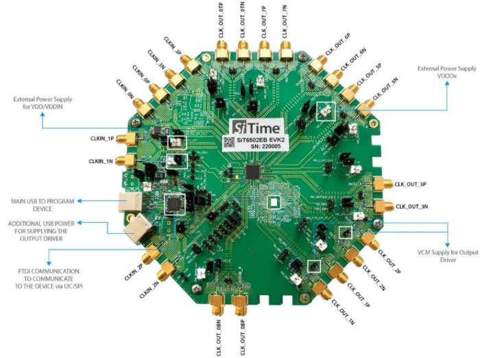
Table 5 lists the Status LEDs on the SiT6502EB EVB in Figure 1.
| Location | Color | Status Function Indication |
|---|---|---|
| D5 | Blue | 5V Main USB Power |
| D6 | Blue | 5V Additional USB Power |
| D12 | Green | FTDI_5V_Power |
| D13 | Green | FTDI_3.3V_Power |
*Note: All LEDs are illuminated when corresponding voltages are present.
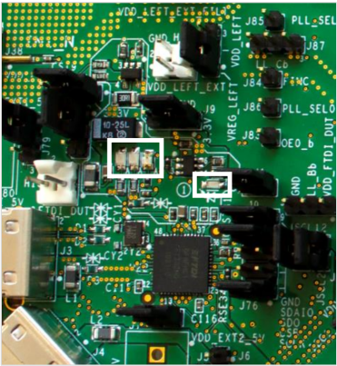
Figure 1. Status LEDs
9. SiT6502EB Power Supplying
Device under Test (DUT) Analog supplying voltage (VDDIN) and DUT outputs supplying voltages (VDDOx) on the SiT6502EB are configured to 3.3 V by default, whereas DUT PLLs supplying voltage VDD supply is configured to 1.8 V. The on board supplies/LDO’s are configurable to 1.8 V, 2.5 V and 3.3 V with the Jumper option as shown in Figure 2. Please refer to SiT95147 datasheet for configuring the supply voltages on the VDDIN/VDD and VDDOx pins and to the Table 6 for on board configuration options for SiT95147:
Table 6. SiT6502EB Supply configuration
| Variant | VDD | VDDIN | VDDOx |
| SiT95147 | 2.5 V / 3.3 V | 2.5 V / 3.3 V | 1.8 V / 2.5 V / 3.3 V |
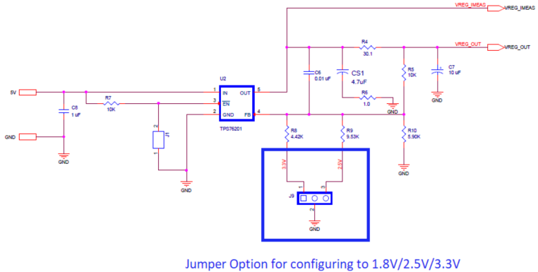
Figure 2. Supply Regulator for VDDIN/VDDOx
Note: For changing the VDDIN (J9) and VDDOx Supply, connect the corresponding Jumpers to below settings:
- 3.3 V – Connect the 3-Pin Jumper from 1 to 2.
- 2.5 V – Connect the 3-Pin Jumper from 2 to 3.
- 1.8 V – Remove the Jumper. There is a provision for connecting external supplies after bypassing the on board regulators for all the supplies as shown in Figure 3.
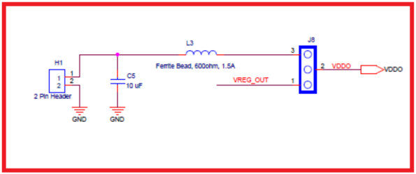
Figure 3. External Supply Connection Provision
PLLs supply circuitry is shown in Figure 4.
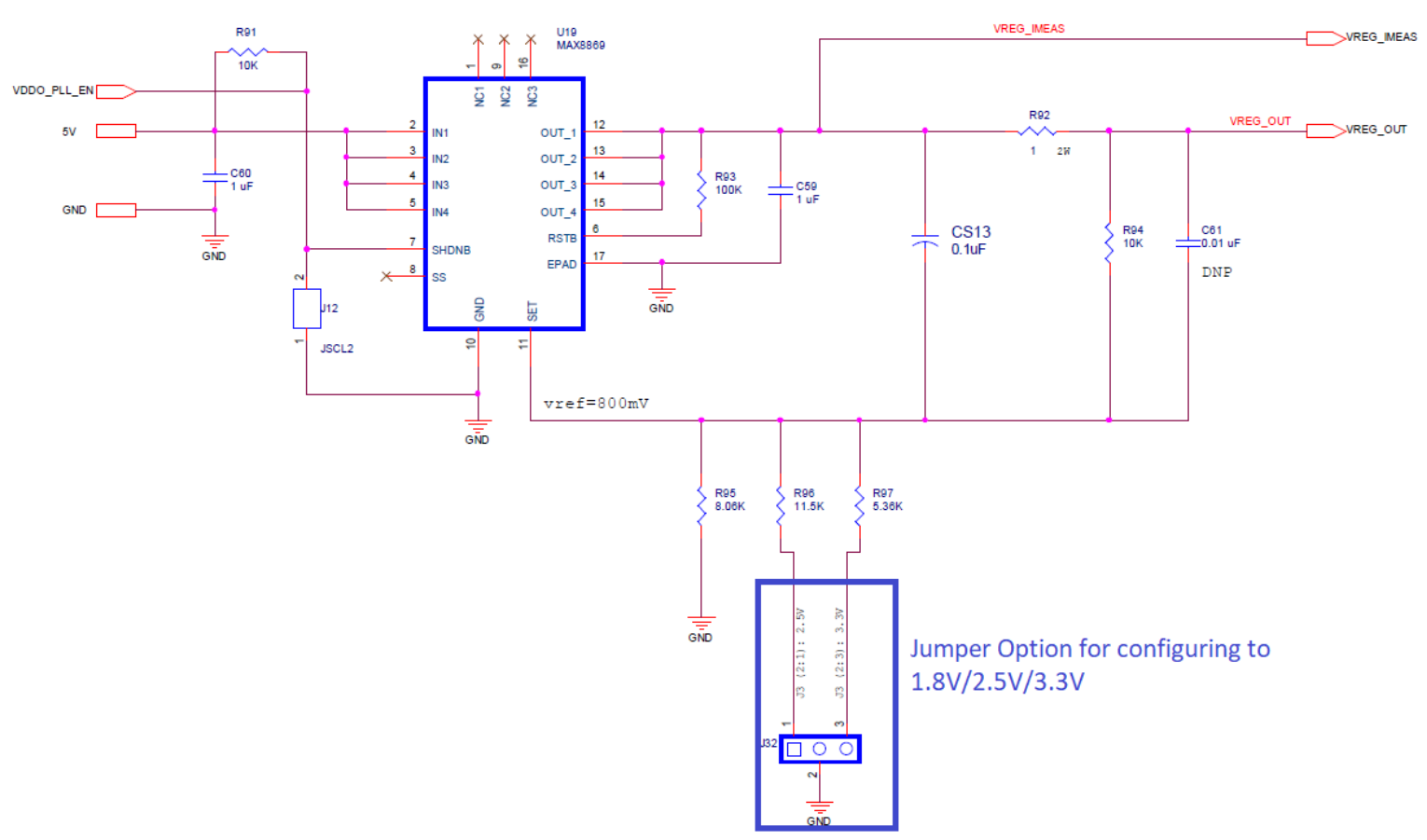
Figure 4. Supply Regulator for
Note: For changing the VDD (J32) Supply, connect the Jumper to below settings:
- 3.3V – Connect the 3-Pin Jumper from 2 to 3.
- 2.5V – Connect the 3-Pin Jumper from 1 to 2.
- 1.8V – Remove the Jumper.
10. I2C/SPI Mode Connection
The 10 pin Header J76 (Figure 5) is mainly used for configuring the SiT6503EB into I2C and SPI Mode (I2C Mode is default one).
For I2C Mode of Operation:
- SCLK_OUT is shorted to SCLK in J76
- SDAIO_OUT is shorted to SDAIO in J76
- CSB_OUT is shorted to CSB in J76
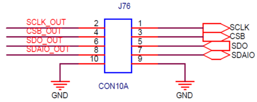
Figure 5. Supply Regulator for PLLs
For SPI Mode of Operation:
- SCLK_OUT is shorted to SCLK in J76.
- SDAIO_OUT is shorted to SDAIO in J76.
- CSB_OUT is shorted to CSB in J76.
- SDO_OUT is shorted to SDO in J76.
- JSCL1 Jumper should be removed.
- JVDD1 Jumper should be changed from (2 to 3) to (1 to 2).
- J73 Jumper should be changed from (1 to 2) to (2 to 3).
11. Clock Inputs
The SiT6502EB has eight inputs (4 differential pairs) with SMA connectors (IN0_P, IN0_N, IN1_P, IN1_N, IN2_P, IN2_N, IN3_P, IN3_N) for receiving external clock signals. All input clocks are AC-coupled and 50Ω terminated as shown in Figure 6 below. This represents four differential input clock pairs. Single-ended clocks can be used by driving the ‘P’ side of the differential pair with the ‘N’ input floating. Figure 6 shows the Input Clock Termination Circuit for one of the 4 pairs.
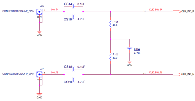
Figure 6. Input Clock Termination Circuit
12. Clock Outputs
When shipped from factory, each of the twenty output drivers (8 differential pairs) is AC-coupled to its respective SMA connector – this is the default configuration. The output clock termination circuit is shown in Figure 7 below. If dc coupling is required, the corresponding 0.1 uF AC coupling capacitor can be replaced with a zero Ω resistor. Figure 7 shows Output Clock Termination Circuit for one of the 8 output pairs.
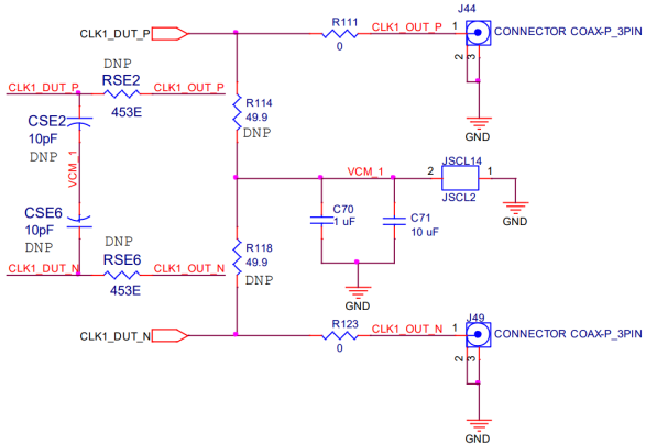
Figure 7. Output Clock Termination Circuit
12.1 Output Differential Termination
LVDS (default configuration), LVPECL, HCSL, and CML differential signaling types can be supported by changing the output termination circuits.
12.1.1 LVDS, CML
The board is shipped to support LVDS, CML in its default differential. The signals are AC coupled with ceramic 0.1 uF capacitors instead of the corresponding series resistors RSExx (Refer to Table 7) which are not populated.
Table 7. Output Port RSExx Resistors
| Output Port # | 1 | 2 | 3 | 5 | 6 | 7 | 0B | 0T |
|---|---|---|---|---|---|---|---|---|
| 0.1 uF capacitors | RSE2 RSE6 |
RSE4 RSE7 |
RSE3 RSE8 |
RSE9 RSE13 |
RSE11 RSE15 |
RSE12 RSE16 |
RSE17 RSE19 |
RSE18 RSE20 |
Output termination resistors as shown in Table 8 are not populated.
Table 8. Output Port Not Populated Resistors
| Output Port # | 1 | 2 | 3 | 5 | 6 | 7 | 0B | 0T |
|---|---|---|---|---|---|---|---|---|
| Not Populated Resistors | R114 R118 |
R115 R119 |
R116 R120 |
R130 R134 |
R131 R135 |
R132 R136 |
R143 R145 |
R144 R146 |
12.1.2 LVPECL
For LVPECL output configuration ceramic capacitors 0.1 uF are placed instead of correspondent series resistors RSExx (Refer to Table 7). Termination resistor values depending on the output driver VDD level are shown in Table 9.
Table 9. Output Port Termination Resistors for LVPECL
| Output Port # | 1 | 2 | 3 | 5 | 6 | 7 | 0B | 0T |
|---|---|---|---|---|---|---|---|---|
| Resistors | R114 R118 |
R115 R119 |
R116 R120 |
R130 R134 |
R131 R135 |
R132 R136 |
R143 R145 |
R144 R146 |
| VDD, 3.3V | 150 Ω | 150 Ω | 150 Ω | 150 Ω | 150 Ω | 150 Ω | 150 Ω | 150 Ω |
| VDD, 2.5V | 120 Ω | 120 Ω | 120 Ω | 120 Ω | 120 Ω | 120 Ω | 120 Ω | 120 Ω |
Also, ensure that jumpers JSCLxx as per Table 10 are populated to allow path to GND.
Table 10. Output Port Jumpers to GND
| Output Port # | 1 | 2 | 3 | 5 | 6 | 7 | 0B | 0T |
|---|---|---|---|---|---|---|---|---|
| Jumpers to GND | JSCL14 | JSCL15 | JSCL16 | JSAL18 | JSCL19 | JSCL20 | JSCL21 | JSCL22 |
For HCSL output configuration series resistors RSExx (Refer to Table 7). 33 Ω should be used for each output port. Please note each lane per pair should be terminated by 50 Ω to GND on the receiver side.
13. Quick Start
- Install Time Master for Clocks GUI on your Windows PC
- Confirm jumpers are installed as shown in Table 3
- Connect a USB cable from SiT6502EB, J3 to your PC
- Launch the Time Master for Clocks GUI
- Refer to the accompanying Time Master for Clocks SW User Manual to configure your frequency plan on the SiT6502EB
- Default Output Driver Configuration is LVDS and Output Driver Supplies are configured to 3.3 V
- Default VDD Supply on the EVB is configured to 1.8V and default VDDIN supply on the EVB is configured to 3.3 V
- The FTDI chip on the EVB is configured to I2C as the default communication protocol
- EVB default configuration is shown in Figure 8.
The general guidelines for single USB power supply operation are listed below:
- Use either a USB 3.0 or USB 2.0 port. These ports are specified to supply 900 mA and 500 mA respectively at +5V
- If you are working with a USB 2.0 port and you are current limited, turn off enough DUT output voltage regulators to drop the total DUT current ≤ 470 mA.
Note: USB 2.0 ports may supply > 500 mA. Provided the nominal +5V drops gracefully by less than 10%, the EVB will still work
Appendix A: EVB Schematic Diagrams
EVB Top Level Diagram
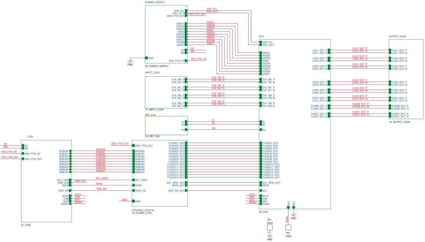
Figure A1. SiT6502EB Top Level Diagram
VDDS Supply
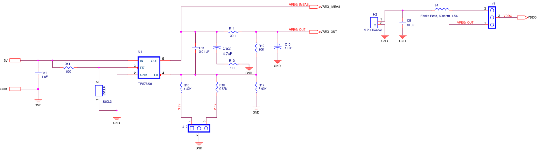
Figure A2. SiT6502EB VDDS Supply Diagram
Power Supply
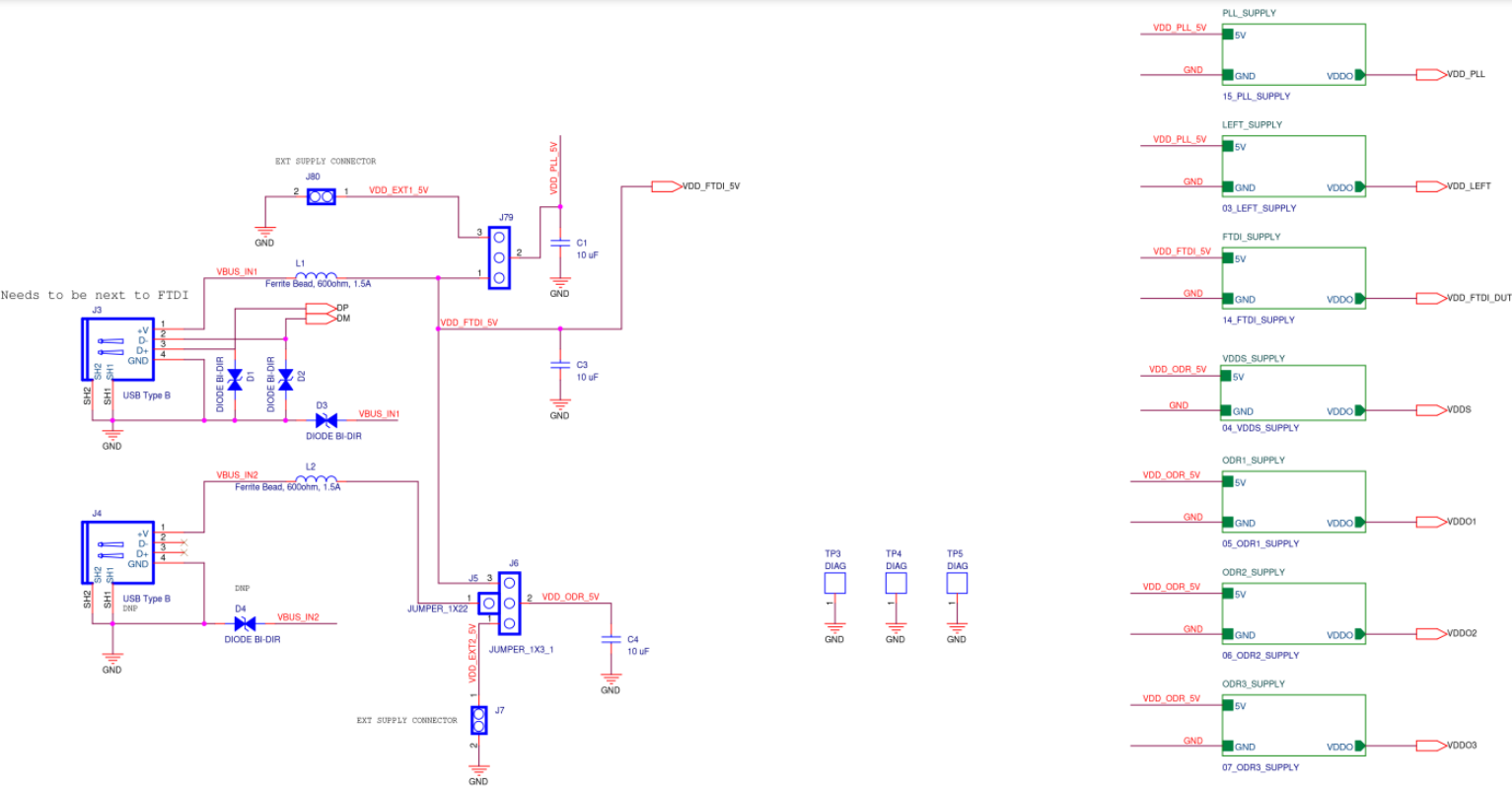
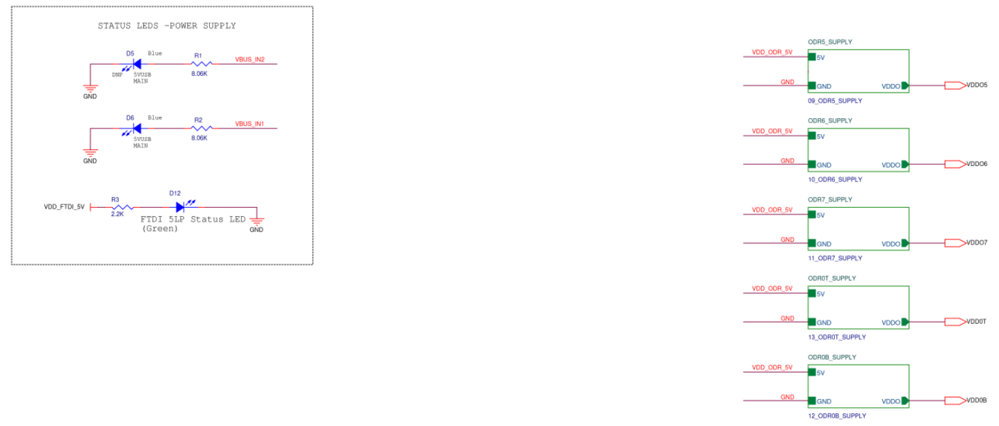
Figure A3. SiT6502EB Power Supply Diagram
Left Supply
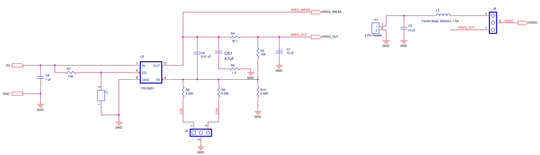
Figure A4. SiT6502EB Left Supply Diagram
ODR1 Supply
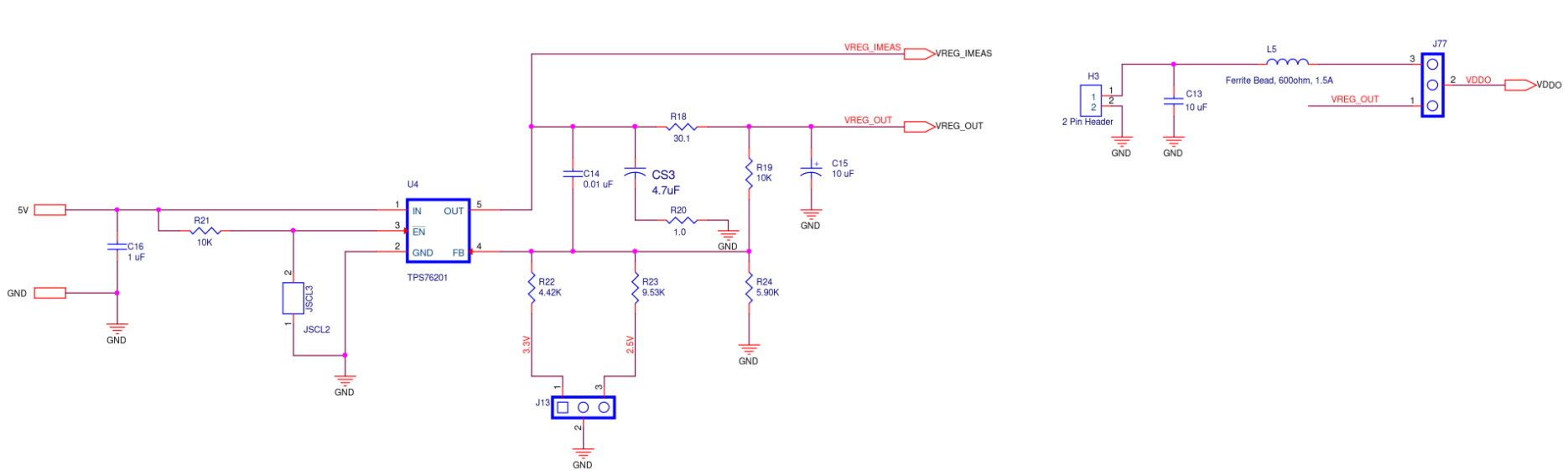
Figure A5. SiT6502EB ODR1 Supply Diagram
ODR2 Supply
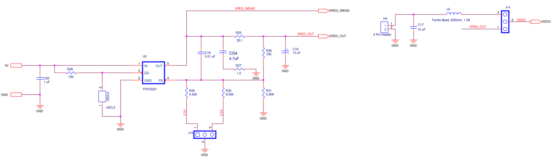
Figure A6. SiT6502EB ODR2 Supply Diagram
ODR3 Supply

Figure A7. SiT6502EB ODR3 Supply Diagram
ODR5 Supply
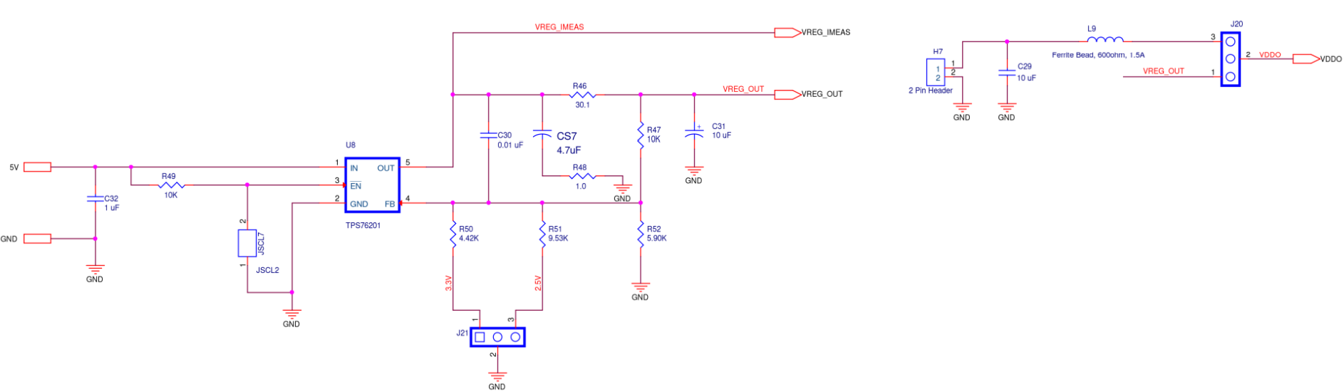
Figure A8. SiT6502EB ODR5 Supply Diagram
ODR6 Supply
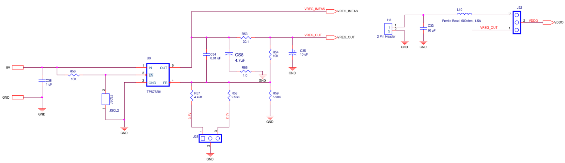
Figure A9. SiT6502EB ODR6 Supply Diagram
ODR7 Supply

Figure A10. SiT6502EB ODR7 Supply Diagram
ODR0B Supply
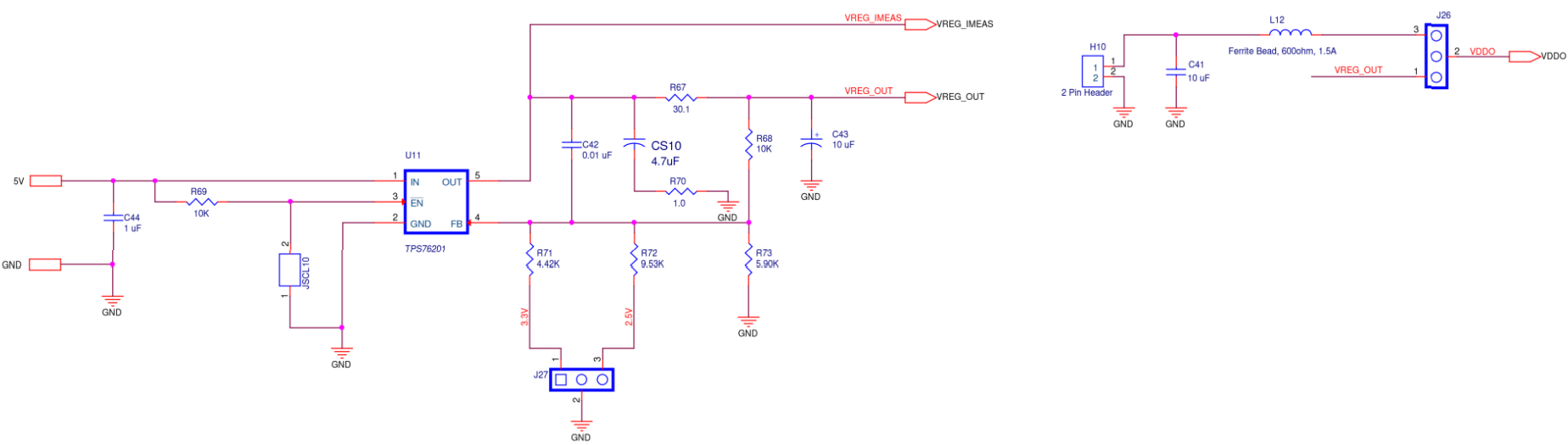
Figure A11. SiT6502EB ODR0B Supply Diagram
ODR0T Supply
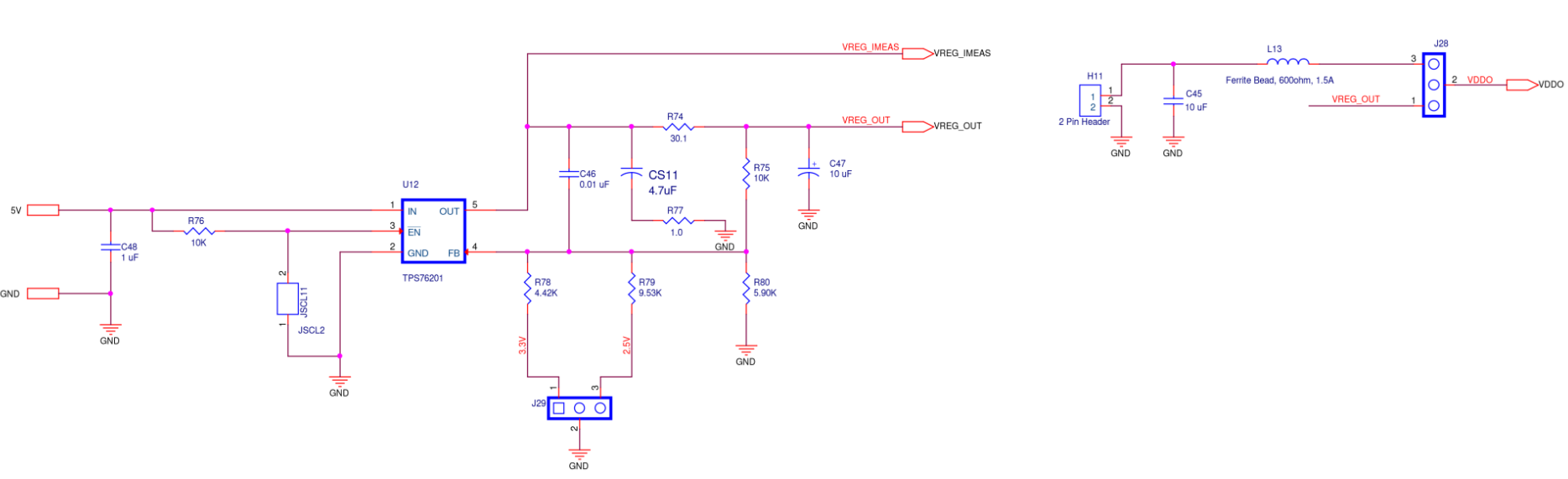
Figure A12. SiT6502EB ODR0T Supply Diagram
FTDI Supply
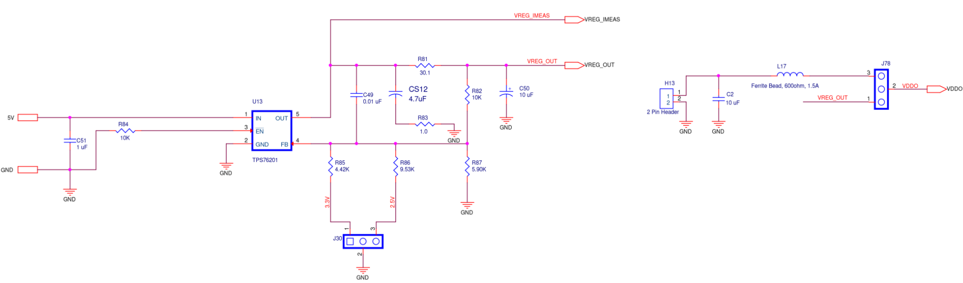
Figure A13. SiT6502EB FTDI Supply Diagram
PLL Supply
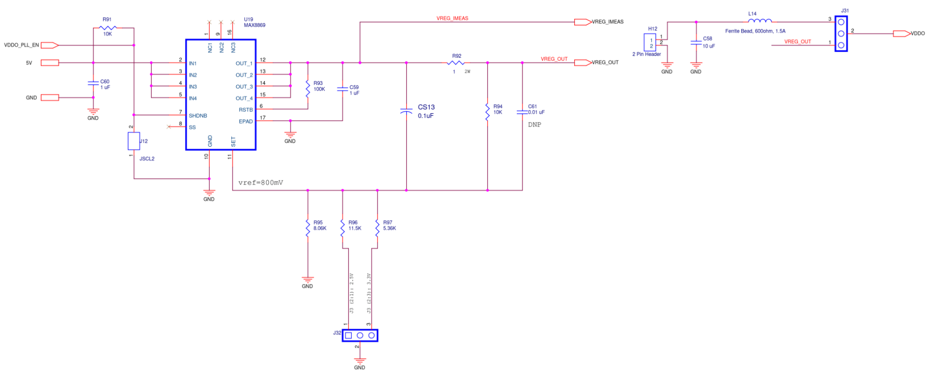
Figure A14. SiT6502EB PLL Supply Diagram
INPUT CLKS
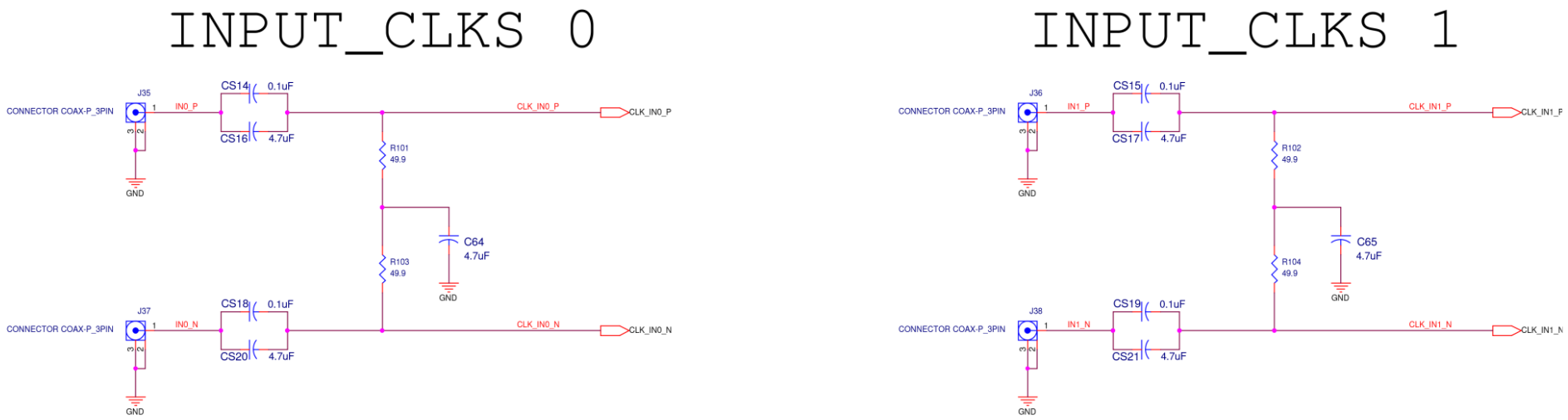
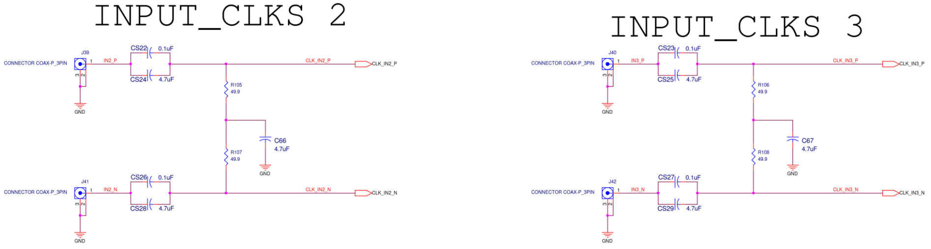
Figure A15. SiT6502EB INPUT CLKS Diagram
OUTPUT CLKS
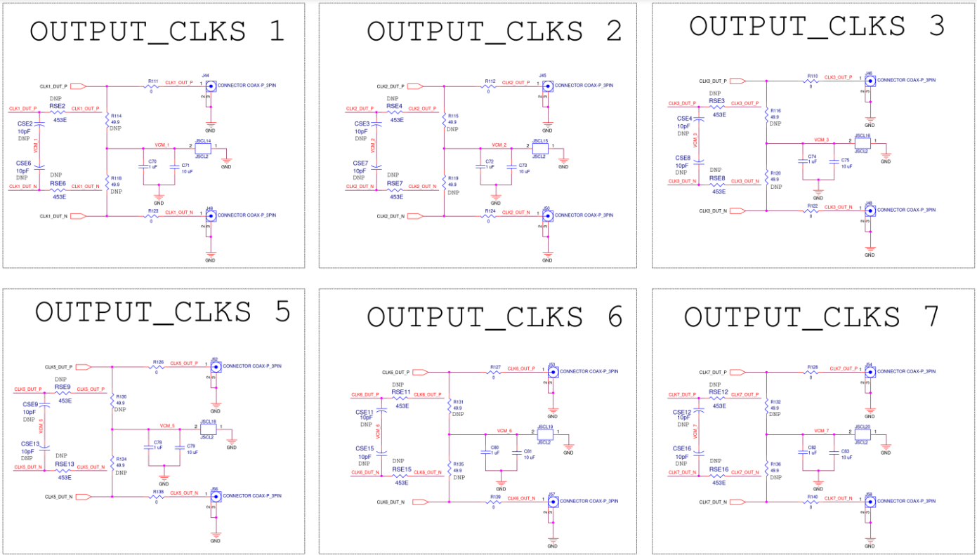
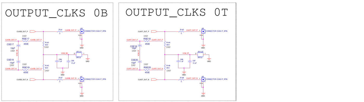
Figure A16. SiT6502EB OUTPUT CLKS Diagram
STATUS LEDS – 2
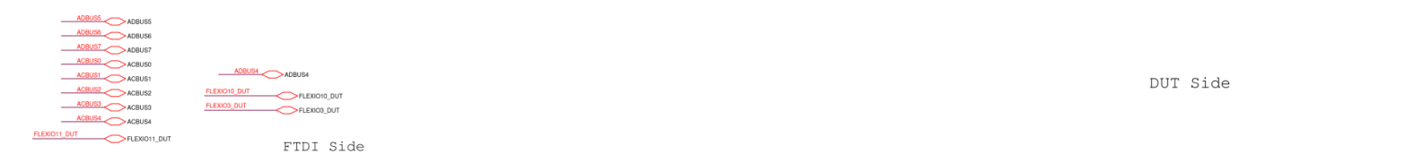
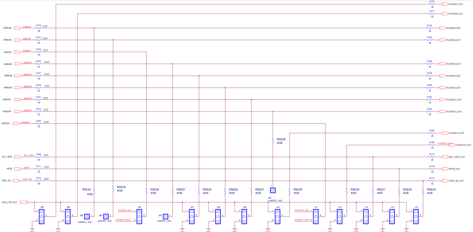
Figure A17. SiT6502EB STATUS LEDS
QFN SiT95147 EVB
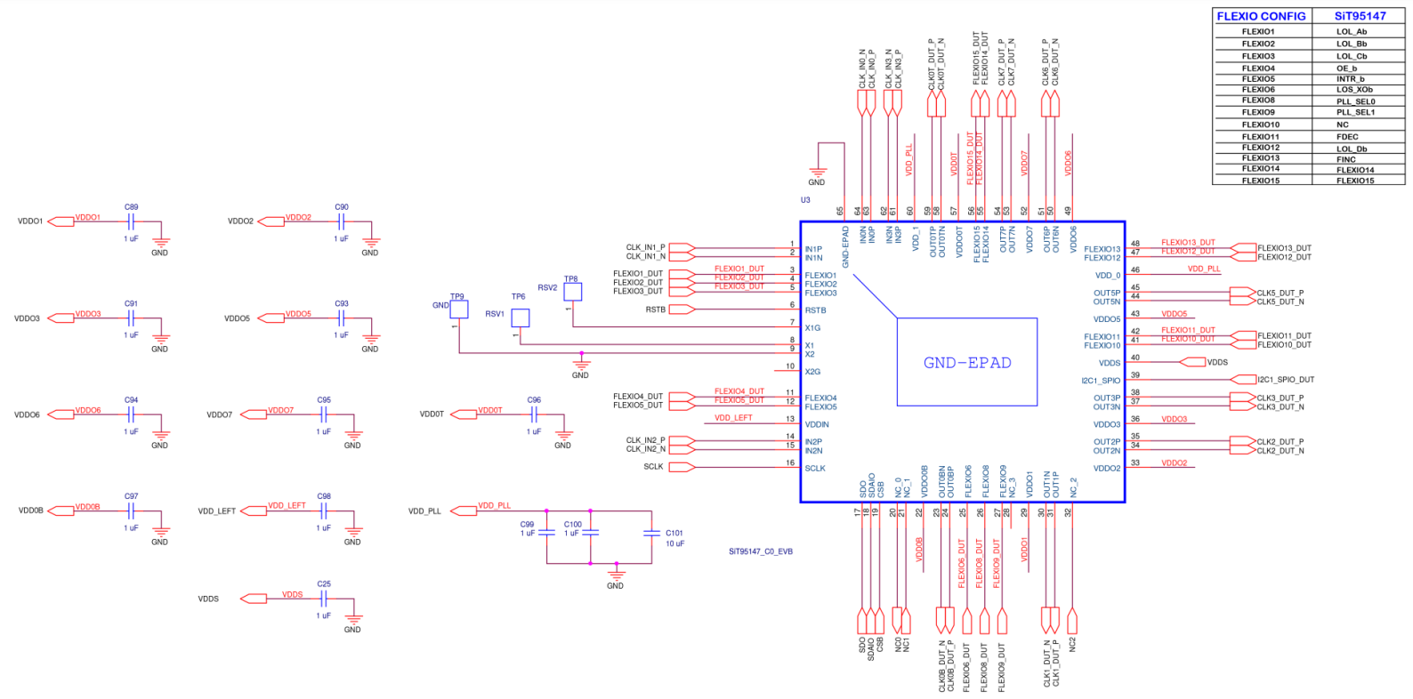
Figure A18. QFN SiT95147 EVB Diagram
FTDI
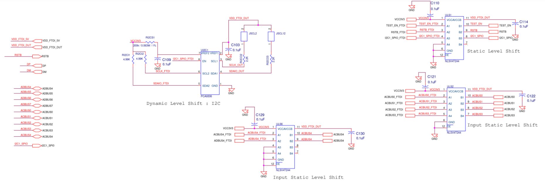
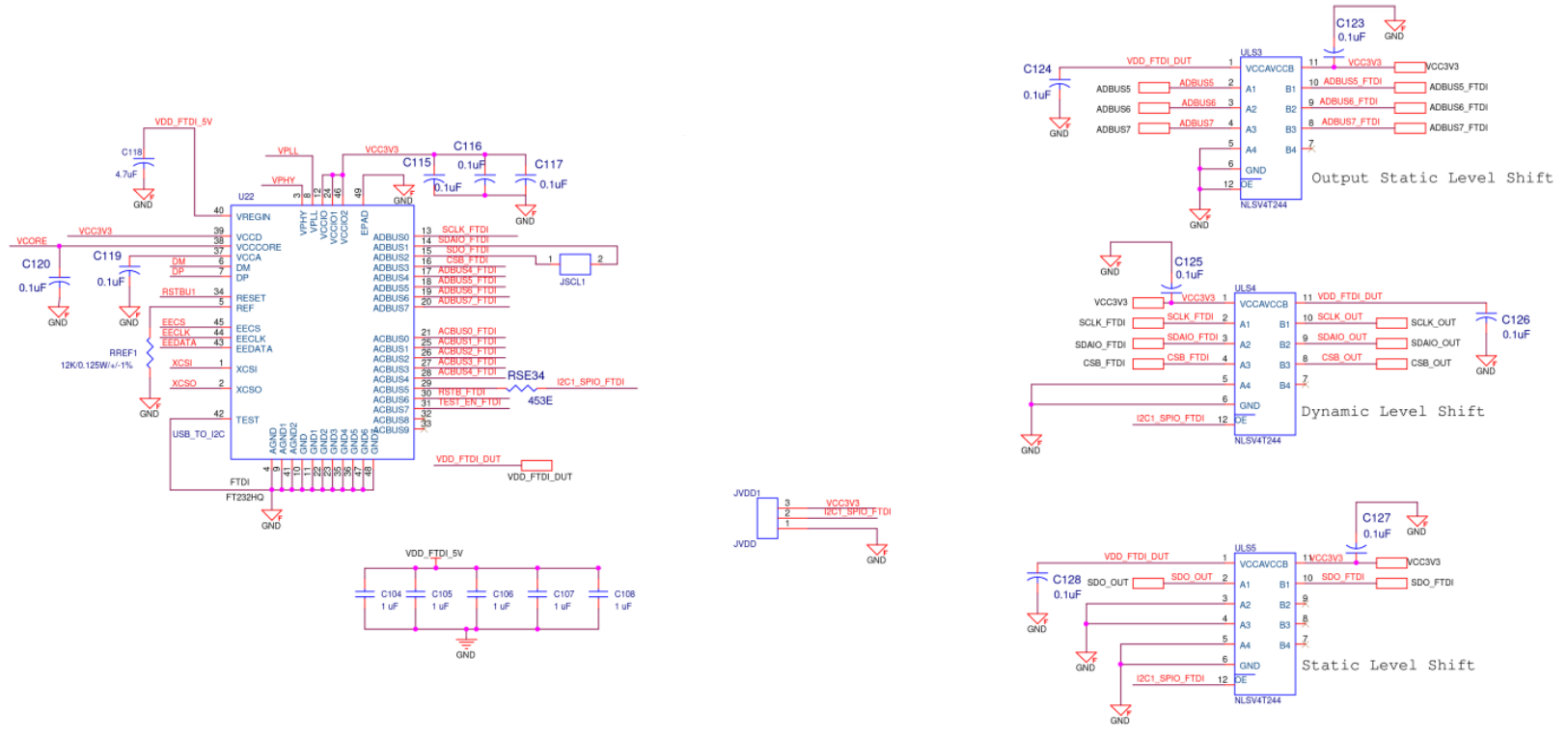
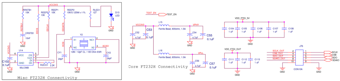
Figure A19. SiT6502EB FTDI Diagram
Appendix B: EVB Top View
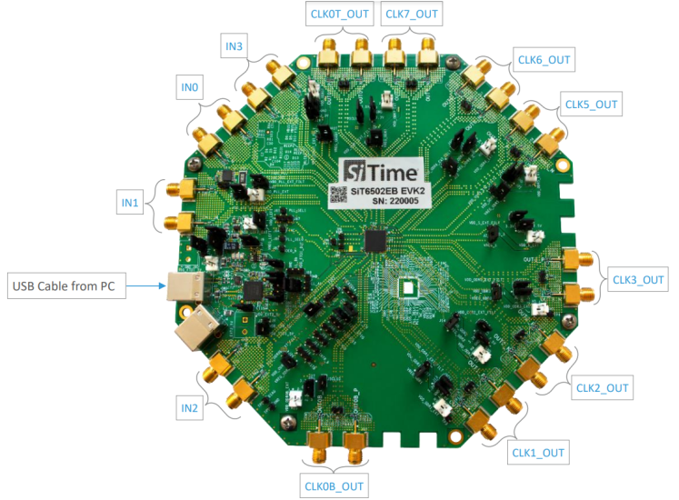
Figure A20. SiT6502EB Top View