Contents
3. Methods of Phase Noise Measurement
4. Connecting the Signal to a Phase Noise Analyzer
4.1 Signal Level and Thermal Noise
4.2 Active Amplifiers and Probes
4.3 Oscillator Output Signal Types
4.3.2 Single-Ended Clipped Sine
5. Setting up a Phase Noise Analyzer
1. Introduction
Phase noise is one of the fundamental metrics for oscillators. An experienced engineer can tell a lot about the quality of an oscillator and whether it fits the application by looking at the phase noise plot. RF engineers focus on the phase noise levels at certain carrier offset frequencies to make sure that the required modulation scheme can be supported. Professionals designing high speed serial links like 40GbE will apply a band pass filter to phase noise of a reference clock, integrate it, and convert it to phase jitter to predict the bit error rate of a system.
This application note starts with a brief theoretical overview of phase noise and methods of phase noise measurement, and then focuses on practical phase noise measurement recommendations such as properly connecting a signal under test to the instrument, setting up the phase noise analyzer, and choosing appropriate settings. All measurements in this document are taken with a Keysight E5052B phase noise analyzer which is one of the most common instruments in North America for measuring phase noise.
2. What is phase noise
Phase noise is a frequency domain representation of short term phase instabilities of a signal. Phase noise is typically described as a single sideband (SSB) phase noise and denoted as L(f). The classical definition of phase noise is the ratio of a power spectral density measured at an offset frequency from the carrier to the total power of the signal. For practical purposes this definition has been slightly modified so that power spectral density measured at an offset frequency from the carrier is referenced to the carrier power, not to the total integrated signal power (Figure 2-1).
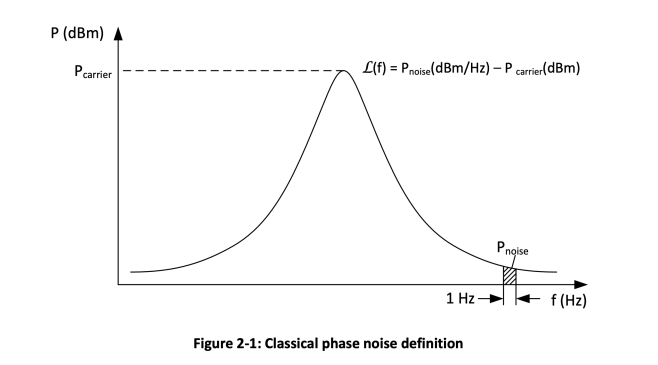
The classical definition is convenient when measuring phase noise with a spectrum analyzer, but it combines both amplitude and phase noise effects. It also has limitations for signals that have high phase noise. The classical definition is generally useful for signals with peak-to-peak phase deviation that is much less than 1 radian. It also can never be greater than 0 dB, since the noise power in the signal cannot be larger than the total power of the signal.
More recently, phase noise has been redefined as half of the power spectral density of phase fluctuations L(f) = SΦ(f)/2. An ideal sinewave can be represented as f(t) = A∙sin(ωt + φ). A Sinewave with phase noise can be represented as f(t) = A∙sin(ωt + φ(t)), where φ(t) is the phase noise. Then SΦ(f) is the power spectral density of φ(t). When defined this way, phase noise is separated from amplitude noise. It can also be larger than 0 dB which means that the phase variations are greater than 1 radian.
3. Methods of phase noise measurement
There are two widely-used phase noise measurement methodologies. The first one utilizes a power spectrum measurement with a spectrum analyzer and the classical definition of the phase noise. The signal spectrum is measured with a certain resolution bandwidth. Then the phase noise is calculated as shown in Figure 2-1. The second methodology is compatible with the most recent phase noise definition through SΦ(f) and uses phase detector techniques. The basic principle of this method is that the signal under test is compared with the reference signal using a phase detector. The output of a phase detector is proportional to the phase difference between its inputs (Figure 3-1).
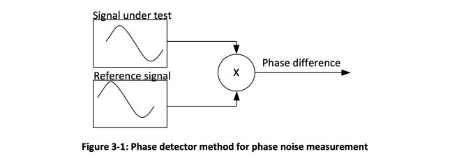
The phase detector method has many varieties. The Keysight E5052B analyzer implements two different variations of this method that are called Normal and Wide in the instrument settings.
The Normal mode is a PLL method that uses a PLL to lock the reference oscillator to a signal under test. This is done to keep the reference signal and the source signal at 90° phase difference on the phase detector inputs. The output from the phase detector is sampled with an ADC and SΦ(f) is calculated using fast Fourier transform (FFT).
In Wide measurement mode, the E5052B uses a so-called heterodyne (digital) discriminator method. It uses an analog mixer to convert the signal under test to an intermediate frequency (IF) which is then sampled with an ADC. The phase detector is implemented in DSP which compares the signal with the delayed version of itself. The output from the phase detector is filtered with a digital low-pass filter to separate the phase difference component from the high frequency component. This time domain digital signal, which represents phase noise, is then run though FFT and normalization in DSP.
The Normal mode is used for stable clock sources. It offers the best sensitivity and wide offset coverage. Wide mode is recommended for signals that have a high level of close to carrier phase noise. Crosscorrelation can be used to improve measurement sensitivity of the heterodyne (digital) discriminator method, especially at close in offsets.
4. Connecting the signal to a phase noise analyzer
4.1 Signal level and thermal noise
Thermal noise is the electronic noise generated by thermal movement of charge carriers in a conductor. It’s expressed as a mean noise power per Hz of bandwidth at a given temperature. The higher the temperature of the resistor, the higher the kinetic energy of charge carriers, and this results in higher noise at higher temperature. Thermal noise is broadband in nature and has an approximately flat frequency spectrum.
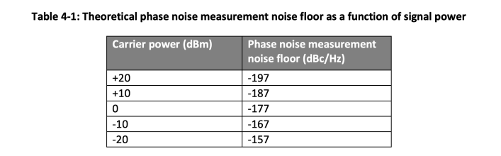
Thermal noise can limit the phase noise measurement noise floor for weak signals. Thermal noise at room temperature is -174 dBm/Hz. The phase noise power portion in thermal noise is 3 dB less than total power resulting in -177 dBm/Hz at room temperature. The theoretical noise floor of phase noise measurement is the difference between the carrier signal power and the phase noise portion of the thermal noise. Table 4-1 shows theoretical phase noise measurement noise floor for input signals of different power levels.
4.2 Active amplifiers and probes
An active amplifier might be required to route a signal under test to a phase noise analyzer, for instance when a signal is too weak to be directly connected to a 50-Ω input of the instrument. A typical example is a clipped sine output type that can be often seen in precision TCXOs and OCXOs. Clipped sine output drivers are relatively high impedance and cannot directly drive a 50-Ω load. Another example is measuring phase noise on a customer board without loading the circuit.
Any active amplifier has its own noise figure and adds noise to the source signal as the signal passes through the amplifier. As a result, the signal-to-noise ratio at the output of the amplifier is reduced as compared to the input signal. If the signal under test has to be amplified or buffered before connecting it to a phase noise analyzer, the noise figure of the amplifier has to be considered to ensure that the noise added by the amplifier is negligible.
Active probes provide a convenient way of accessing a signal in a system or on an evaluation board. They add minimum parasitic load to a system and come with a number of accessories that make it easy to connect to a trace, pin, probe point, or other feature on the board. Active probes are designed primarily for accurate waveform measurement of high bandwidths signals. As a result, there are two major problems when using active probes for a phase noise measurement:
- Active probes are high bandwidth and add a significant amount of broadband noise to the signal.
- To ensure high bandwidth capability of a probe, the amplifier in a probe head divides down the signal level. This means the power of a signal on a phase noise analyzer input is reduced and the measurement noise floor is degraded due to the thermal noise.
It is not recommended to use active probes for phase noise measurements.
4.3 Oscillator output signal types
Oscillators can have different output signaling types. The two major categories are single ended signals and differential signals. Single ended signals carry a clock signal on a single wire with respect to the common ground. Differential signals use two signal wires that carry identical clock signals that are 180° out of phase with each other.
This chapter will provide recommendations for connecting the most common signal types to a phase noise analyzer.
4.3.1 Single ended LVCMOS
LVCMOS is a single ended output type that typically has output levels from 0V to VDD. Output impedance often ranges between 20Ω and 40Ω. An LVCMOS output can often be directly connected to a 50-Ω input of a phase noise analyzer, but there are couple things to keep in mind:
- The connection must be made with a shielded 50-Ω cable and it’s better to keep the length short (<= 3 ft) to minimize the insertion loss and consequent signal attenuation.
- The input to a phase noise analyzer has a 50-Ω termination, and loading an oscillator with a 50- Ω load can draw a significant amount of current from the output driver. This power dissipation slightly increases internal die temperature. Another impact of high current draw from the driver is the level of harmonic components in the phase noise called spurs. If there are any spurs associated with the output driver impact on the other blocks in the oscillator circuit, then increasing driver current may increase the level of those spurs and they will have larger amplitude than under normal load conditions.
4.3.2 Single ended clipped sine
A clipped sine output is a single ended output with slow rise/fall times and reduced signal levels that can often be encountered with precision TCXOs and OCXOs. The output impedance of such an output is relatively high (kΩ range) and connecting a clipped sine output directly to a 50-Ω input of a phase noise analyzer means the signal power is low and the thermal noise will significantly limit the measurement noise floor. For example, a clipped sine output with source impedance of 1 kΩ and peak-to-peak voltage of 1V will deliver about -20 dBm power to the 50-Ω instrument input. This results in a theoretical measurement noise floor of -157 dBc/Hz which is not acceptable for a clock signal that is supposed to reach -170 dBc/Hz at 5 MHz offset from the carrier.
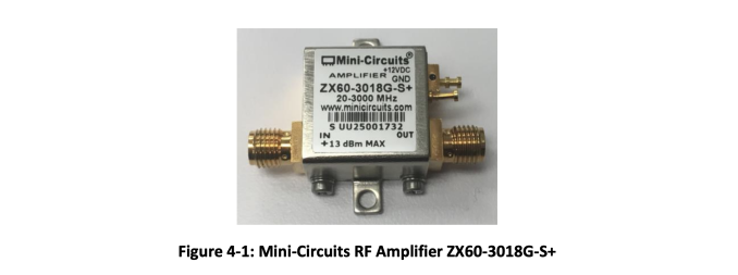
To avoid this situation, the signal power must be boosted to an acceptable level. One of the options is to use a low noise RF amplifier, like Mini-Circuits ZX60-3018G-S+ (Figure 4-1). It has SMA input and SMA output and can easily be injected in to the measurement setup.
4.3.3 Differential outputs
The most common differential signaling types for oscillators are LVPECL and LVDS. Less prevalent but still used in some applications is HCSL. Differential outputs have a number of advantages: common mode noise reduction, resistance to noise coupling, excellent power supply noise rejection, and high frequency capability.
Phase noise analyzers usually have single ended input, but differential interfaces have two outputs. The easiest way to connect a differential output to a single ended instrument which has a 50-Ω input is to connect one of the outputs directly to an instrument and terminate the other one with 50 Ω to ground to balance the drive currents. The two drawbacks of that approach are that common mode noise is not cancelled out which can increase the noise floor and half of the signal power is lost. Additionally, as discussed previously, a weaker signal leads to a higher impact of the thermal noise.
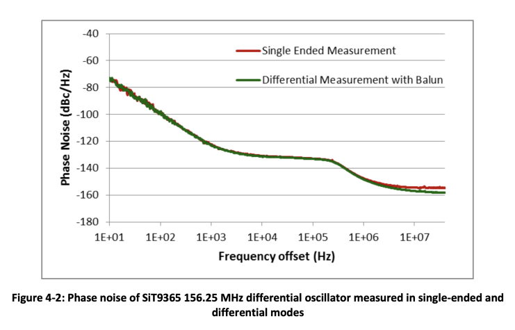
A better solution is to use a balanced-unbalanced converter balun to convert from differential signal to single ended, and then connect to a phase noise analyzer. A balun is a high frequency transformer, where the differential signal is connected to opposite sides of a primary winding and the single ended signal is picked out of the secondary winding. Figure 4-2 illustrates phase noise of a SiT9365 differential oscillator measured in single ended mode (one of the outputs connected to a phase noise analyzer) and in differential mode using JTX-2-10T RF transformer form Mini-Circuits as a balun. It can be observed that the single ended measurement has higher noise floor.
5. Setting up a phase noise analyzer
5.1 Automatic setup
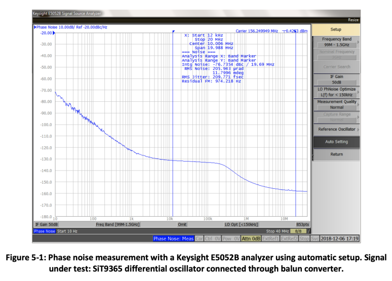
Most phase noise measurement instruments have an automatic setup feature. Its purpose is to select the most optimal instrument settings for the given input signal. When automatic setup is used in the Keysight E5052B phase noise analyzer, the instrument detects the power level and frequency of the input signal and automatically sets up several settings, including input attenuation, intermediate frequency gain, and frequency range. All other settings, like start/stop frequency, averaging, or crosscorrelation, depend on the measurement needs and are not set by the automatic setup. Figure 5-1 shows phase noise measurement made with a Keysight E5052B analyzer using automatic settings. The signal under test is a SiT9365 differential oscillator connected through a balun converter.
5.2 Setting input attenuation
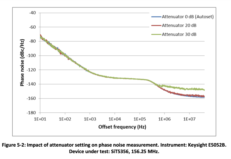
Input attenuation has to be set following the recommendations from the instrument vendor. Too much attenuation may reduce signal power to the point where the thermal noise starts degrading the noise floor. Too little attenuation may lead to circuit overload and bad measurement results. Figure 5-2 illustrates how phase noise measurement noise floor increases as the input attenuator setting is changed from 0 dB, selected by the auto setting function, to 20 dB and 30 dB.
5.3 Averaging
Most of the phase noise analyzers have measurement averaging capability. This feature runs the measurement by the specified number of times and averages the results. It makes the phase noise trace look smoother, but it takes significantly more time.
Figure 5-3 illustrates SiT5356 precision TCXO phase noise measured with a Keysight E5052B analyzer. Two averaging settings have been used: no averaging and 16x averaging. When the instrument applies averaging, more data is available for processing which reduces measurement uncertainty and leads to a better statistical representation of the random noise. The user should ideally try a couple of different averaging settings to find the optimal balance between the measurement speed and quality of the measurement.
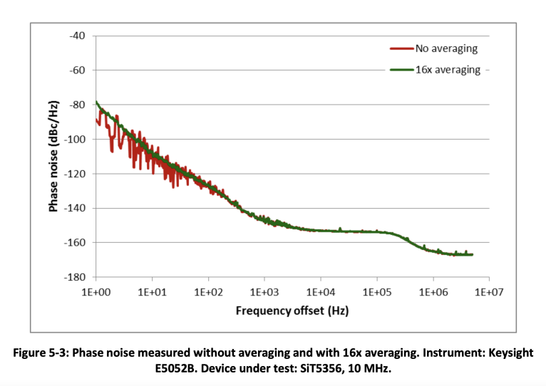
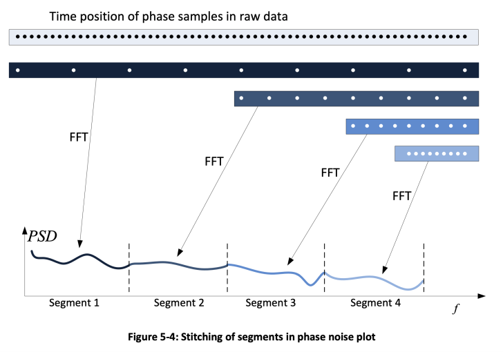
As can be seen from Figure 5-3, both traces with and without averaging are smooth and almost identical at far out offsets, but the trace without averaging looks very “noisy” at close in offsets. This difference is mostly due to the way the Keysight E5052B analyzer processes the data. The raw phase data is collected with high sample rate. Running FFT on the full data set requires a lot of computing resources, so the instrument splits the phase noise plot into fixed segments. This allows using different resolutions for plot segments, so the lower offsets can have higher resolution and the far out offset can have lower resolution. This is very convenient for plotting the data in logarithmic horizontal scale. For example, 1 Hz to 47.7 Hz is the first segment, 47.7 Hz to 190.7 Hz is the next segment, and so on. To compute FFT for the first segment, the full time length of the raw data is used, but the sample rate is reduced by skipping samples. For the next segment, the sample rate is higher than for the first one, but the time duration of the sequence is reduced (refer to Figure 5-4).
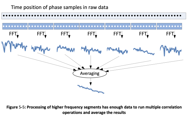
This approach has another benefit. In Figure 5-4 the data used to compute the FFT for segment 4 has the maximum sample rate, but relatively short time duration. This means that the original phase data set can be cut into multiple consecutive data sets, like the one used to compute the FFT in the illustration. Then FFTs can be computed individually for each of the data sets and averaged to get a better measurement for the segment (Figure 5-5). In phase noise analyzer documentation this process is referred to as executing a certain number of correlations since a vector averaging of a number of crosscorrelations is performed. The Keysight E5052 manual specifies how many correlations are applied to each segment of the phase noise plot. This is additional processing that the instrument does automatically and the user has no control over it. This is why a phase noise trace measured with a Keysight E5052B analyzer with no averaging looks smooth at higher offsets, but requires averaging to improve measurement quality at close in offsets.
5.4 Cross-correlation
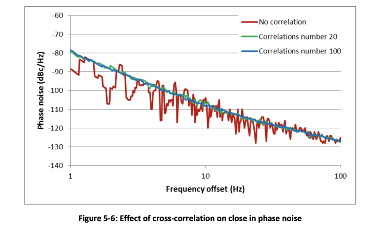
Cross-correlation is another technique to improve phase noise measurement noise floor. The signal under test connected to the phase noise analyzer is split into two measurement channels that consist of a reference source and a PLL system. Cross-correlation is applied between the outputs of these two channels. Noise coming from the signal under test is coherent and therefore not impacted by crosscorrelation operation. Noises from measurement channels are incoherent, so they are reduced by the cross-correlation at the rate of sqrt(M), where the M is number of correlations.

where 𝑁𝑚𝑒𝑎𝑠 is the measured noise, 𝑁𝑆𝑈𝑇 is noise present in the signal under test, 𝑁1 and 𝑁2 are the noises added by measurement channel 1 and channel 2 respectively, and 𝑀 is the number of correlations. Using the cross-correlation setting improves the measurement noise floor. It’s also a way to apply averaging to the phase noise data and smooth out the trace. The drawback is the significantly increased measurement time. Figure 5-6 illustrates how the cross-correlation feature helps to achieve better measurement results at close in offsets.
5.5 Spurs on the phase noise
Spurs are harmonic components in the phase noise spectrum. On a phase noise plot, they look like vertical spikes on the data. The ideal mathematical model of a spur in a frequency domain is a Dirac delta function multiplied by the spur amplitude, so the spur cannot be described accurately through power spectral density expressed in dBc/Hz. The better unit of measure for spurs is dBc.
Random noise is unbounded and the peak-to-peak value increases with the sample size. Deterministic noise is bounded and does not increase with the sample size. Random and deterministic phase noise components have to be considered separately when calculating the impact on system performance.
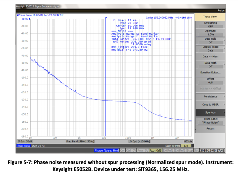
Most of the phase noise measurement instruments have built-in algorithms to detect spurs and process them in a different way in order to separate them from the random noise. Figure 5-7 shows phase noise measured with a Keysight E5052B analyzer in a Normalized mode of spur processing. In this mode, the spurs are not distinguished from the random noise and are processed in the same way as random noise. Figure 5-8 illustrates Omit mode that detects the spurs and removes them from the plot. Figure 5-9 shows the same phase noise measurement in a Power spur mode. This mode detects the spurs, separates them from the random noise and expresses them in dBc units. They are also displayed in a different color than random noise.
It is important to note that when the spurs are displayed in dBc units they may look large and disturbing. In reality they are expressed in different units and cannot be visually compared to the random noise. A good way to get a feel of the spur value in terms of jitter impact is to convert the spur from dBc to time units. The Keysight E5052B analyzer has a feature that allows exporting a spur table. Using the following formula, spur can be converted from dBc to fsrms:

where L(f) is the spur value in dBc and fcarrier is the carrier frequency. The largest spur in Figure 5-9 is about -100 dBc which is the typical performance of a SiTime SiT9365 differential oscillator. Let’s convert it to the RMS jitter:

So the power of the spur is only 14.4 fsrms.
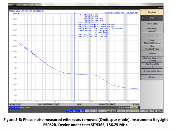
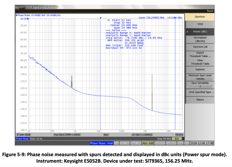
Table 5-1: Revision History
|
Version |
Release Date |
Change Summary |
|
1.0 |
12/14/2018 |
Original doc |
|
1.1 |
|