Contents
2 Lumped versus distributed PCB traces
3 Clock termination recommendations
3.1 Source termination for driving single load
3.2.1 Driving multiple loads lumped at the end of the trace
3.2.2 Driving two transmission lines from one source
3.2.3 Star topology for driving two loads
3.3 Low-pass filter effect when using source termination
Additional Content in the PDF:
References
Appendix A: Signal edge propagation in a series terminated transmission line Appendix
Appendix B: Reflection coefficients Appendix
Appendix C: Output impedances of SiTime parts for different drive strength options
1. Introduction
Clock signals with fast edges see traces on Printed Circuit Boards (PCB) as transmission lines rather than simple wire connections. If the length of PCB trace exceeds certain limit it requires matching of the trace impedance to one or both of the source and load impedances. Impedance mismatch causes signal reflections travelling back and forth the transmission line causing signal distortions such as ringing, overshoots, and undershoots. This application note provides guidelines for proper termination of single-ended traces driven primarily with LVCMOS outputs. This document discusses single-load as well as multiple-load scenarios.
2. Lumped versus distributed PCB traces
Clock source, PCB trace and clock receiver are considered a lumped system if in response to an input signal all points react together with uniform potential. If the response is distributed along the trace the system is called distributed system. The speed of signal propagation in any environment is limited so there can be no perfect lumped system. It is a common practice to compare the length of the PCB trace to effective length of a fastest clock signal edge and use this ratio to judge if for practical purposes the system can be treated as a lumped system. The effective signal edge length in a trace is calculated as:
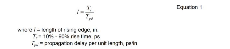
For example, propagation delay in an FR4 PCB trace ranges from 140 to 180 ps/in. Assuming Tpd = 150 ps/in. the effective length of a 1 ns rising edge is 6.7 in.
The circuit behaves mostly in a lamped fashion if the length of the PCB trace is less than or equal to one-sixth (l/6) of the effective length of a signal edge. When comparing to 20% - 80% rise/fall times, the more appropriate ration is l/4 to decide whether a trace can be considered a lumped element. Lumped circuits do not require termination. For example, assuming a clock signal with 1 ns 10%-90% rise time and FR4 PCB material traces longer than 1.1 in. have to be treated as transmission lines.
Tables of rise and fall times of SiTime oscillators for different load options and drive strength settings are available in datasheets for most part families. Select the lowest load option from the datasheet rise/fall time table (usually 5 pF) when using Equation 1 because capacitive load at the receiver side does not impact the rise/fall times at the source when driving a transmission line.
When a clock driver sends an edge into the transmission line, the edge reaches the load after some delay. If the impedance of the load (ZL) is different from the impedance of the transmission line (Zo), a portion of the signal reflects from the load towards the source. Mismatch at the source causes portion of reflected signal reflect back to the load (round-tip reflection). The fraction of the signal that reflects is determined by the reflection coefficients [Appendix B]. Following sections describe termination strategies that can be used to minimize reflections and improve signal integrity when driving single or multiple loads.
3. Clock termination recommendations
This section describes commonly used source termination strategies.
3.1 Source termination for driving single load

Figure 1: Series Termination
Series termination is constructed by inserting a resistor in series with the trace as close to the source as possible (see Figure 1). For proper impedance matching the output impedance of the clock driver plus series termination resistor should be equal to the trace impedance, i.e.:
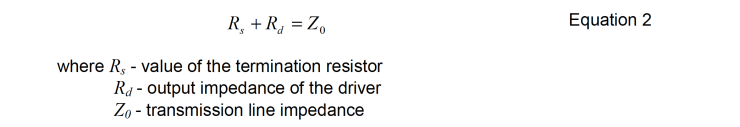
As an example we calculate the value of termination resistor that is suitable for SiT8208 device with default drive strength and operating at 3.3V driving a 60-Ω trace. From the product datasheet [2] table 4 we determine that the default drive strength code is “F”. Using table 1 from the Appendix C we determine that the typical output impedance of SiT8208 device with drive strength code “F” and 3.3V operating voltage is 15.3 Ω. Substituting trace impedance and output impedance into Equation 2 we calculate source termination resistor value Rs = 60 Ω - 15.3 Ω = 44.7 Ω.
With a configuration in Figure 1, the signal from the source will travel along the trace until it reaches the load. Typical loads have very high input impedances (in the range of mega-ohms), so no energy will be absorbed and the entire signal is reflected back to the source. Because the impedance at the source is matched to that of the transmission line, no further reflections will occur. Refer to Appendix A for the detailed diagram of signal propagation in a series terminated transmission line.
SiTime recommends simulating the layout using oscillator IBIS model provided by SiTime. As an example we use Signal Integrity Analysis tool from the Altium Designer software to simulate SiT8208 oscillator driving 5-inch 60-Ω transmission line. Figure 2 shows signal waveforms simulated at the load side. Termination resistor Rs = 43 Ω is chosen to match 60-Ω line impedance. The same value of termination resistor is used to simulate +/-10% trace impedance variations thus taking into account PCB manufacturing spread.
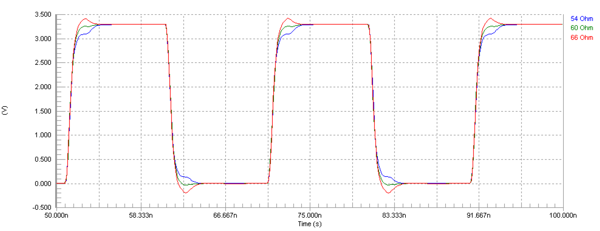
Figure 2: Altium Designer simulation waveform for SiT8208 driving load through 5 in transmission line. Trace impedance – 54, 60, and 66 Ω, supply voltage – 3.3 V, source termination – 43 Ω, load capacitance – 5 pF.
Refer to Appendix C for information about typical output impedances of SiTime single ended oscillators.
3.2 Driving multiple loads
Two or more IC’s on PCB may require an input clock of the same frequency. One method to drive more than one load with a clock is to use fan-out buffers, which require additional board space and power. An alternative is to connect one output to multiple loads.
The preferred way of connecting one output to multiple loads is routing a single transmission line as close to the loads as possible and connecting the loads with short traces using a star connection, so the loads are considered lumped at the end of the trace (3.2.1). This method requires the loads to be close enough to each other.
If the loads are too far from each other to be able to use lumped load configuration then under certain conditions one output can be used to drive two transmission lines going to separate loads (3.2.2). This configuration requires from the output driver higher current drive capability than for driving a single transmission line and is not recommended for use with 1.8V versions of SiT1602 and other devices listed in Table 2 when using 60-Ω and lower impedance transmission lines. It’s recommended to run signal integrity simulation using IBIS models before incorporating this configuration into the design.
Some drivers may not have enough drive capability to handle two transmission lines. If the distance between the oscillator output and the loads is small enough the star topology may be considered (3.2.3).
The output driver of a typical oscillator is not strong enough to drive three or more transmission lines with the impedance of traces that can be easily designed on a PCB (50 – 60 Ω). SiTime does not recommend driving three or more transmission lines from a single driver.
3.2.1 Driving multiple loads lumped at the end of the trace
The easiest scheme of driving multiple loads is when the loads are lamped at the end of the transmission line (Figure 3). It can be achieved if the loads can be placed close enough to the end of the transmission line so that the traces connecting each load to the transmission line are not longer than one-sixth of the effective length of the signal edge. The loads have to be connected in a “star” formation as shown in Figure 3. The value of series termination resistor is calculated the same way as for a single load case (Equation 2).
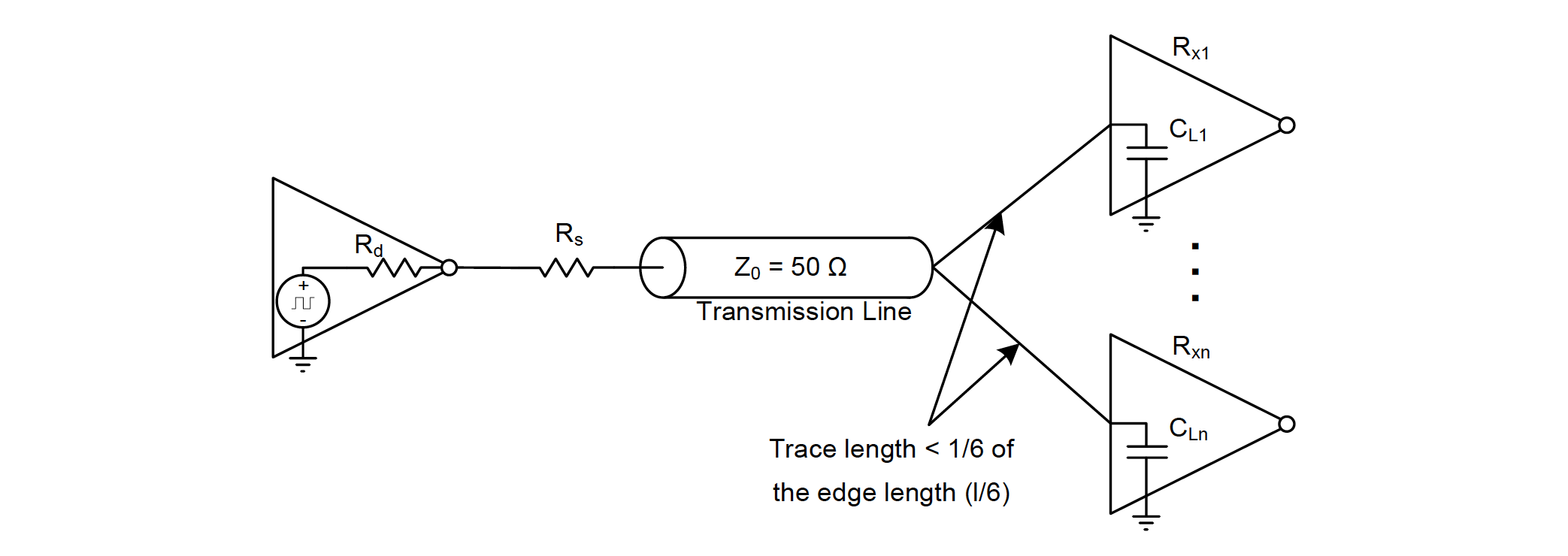
Figure 3: Series termination with multiple loads lumped at the end of the trace
Figure 4 illustrates Altium Designer simulation results of the scheme in Figure 3 for SiT8208- 3.3V oscillator provided that Rs = 43 Ω, CL = 5 pF, number of clock receivers – 2, length of stubs 0.5 in. (~75 ps). If the stubs are too long reflections cause signal integrity issues (see Figure 5).
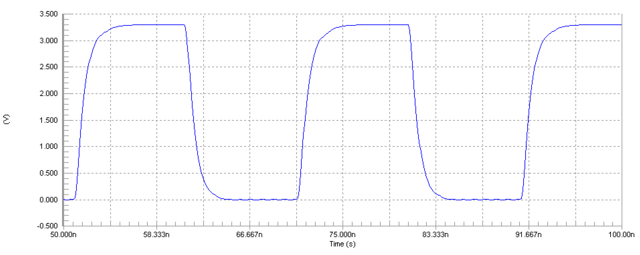
Figure 4: Altium Designer simulation waveform (at the load side) for SiT8208 driving two loads lumped at the end of 5-in. trace. Trace impedance – 60 Ω, supply voltage – 3.3 V, source termination – 43 Ω, load capacitance – 5 pF.
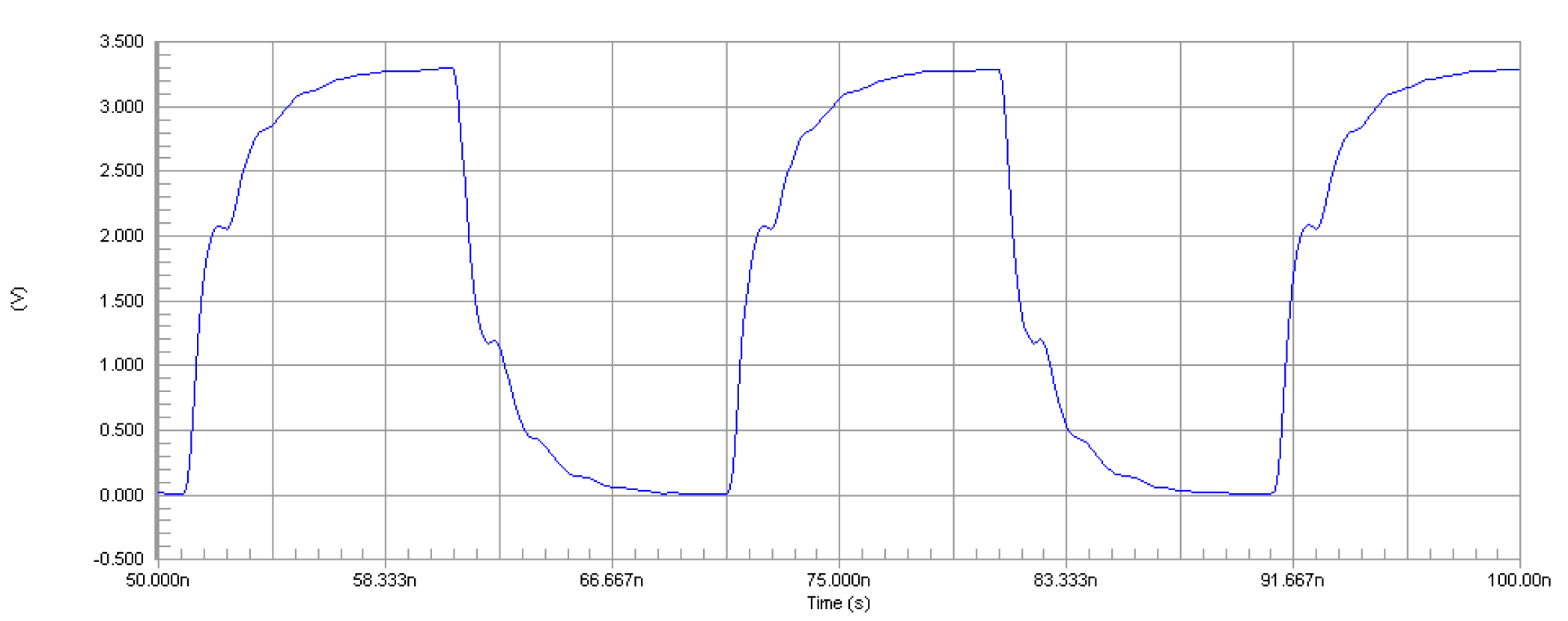
Figure 5: Altium Designer simulation waveform (at the load side) for SiT8208 driving two loads when the trace from the driver splits after 2 in. into two 3-in. sections each connecting to the load. Trace impedance – 60 Ω, supply voltage – 3.3 V, source termination – 43 Ω, load capacitance – 5 pF.
3.2.2 Driving two transmission lines from one source
The clock receivers may not be arranged in a lumped load configuration if the clock receivers are far from each other. In such case, a separate transmission line may be used to deliver the signal to each load. Figure 6 illustrates a configuration that can be used for driving multiple source terminated transmission lines from a single driver.
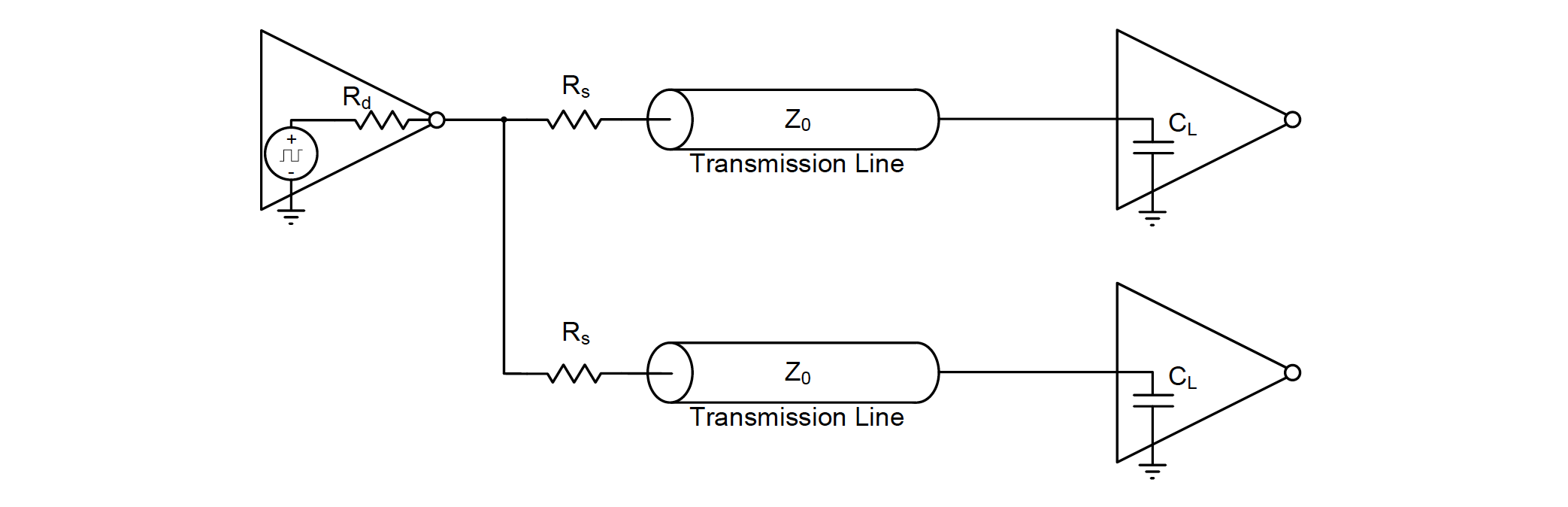
Figure 6: Driving multiple transmission lines from one source
This method is low cost since it requires only one termination resistor per trace and offers full swing signal amplitude at the load side. The following conditions should be met for optimal signal integrity [1]:
1. Clock driver can supply enough peak current during the edge transmission
2. All transmission lines are of the same length
3. Capacitive loads at each receiver side are approximately the same
4. Termination resistors are calculated from Equation 3
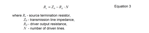
Figure 7 shows Altium Designer simulation results of the scheme in Figure 6 for SiT8208-3.3V oscillator. Source termination resistors are calculated according to the Equation 3. The little dip after the rising edge and the small bump after the falling edge occur mostly due to parasitic capacitances of loads and source driver that cause slight impedance mismatch.
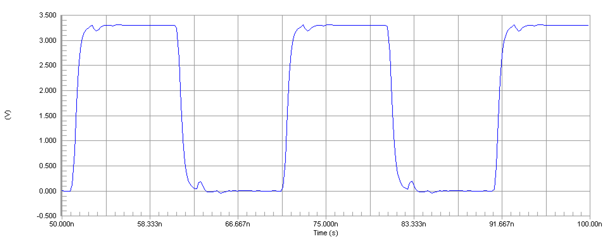
Figure 7: Altium Designer simulation waveform (at the load side) for SiT8208 driving two 5-in. transmission lines. Trace impedance – 60 Ω, supply voltage – 3.3 V, Rs = 15 Ω, CL = 5 pF.
Driving two 50-Ω transmission lines requires stronger driver than for driving two 60-Ω lines. Figure 8 shows Altium Designer simulation results of the scheme in Figure 6 using the same SiT8208-3.3V oscillator, but driving two 50-Ω lines. The source termination resistors are set to zero, but still the source impedance is too high to ensure as good signal integrity as has been achieved in Figure 7. It is recommended to select stronger drive strength option for the SiT8208 oscillator than the default drive strength which has been used for the simulation.
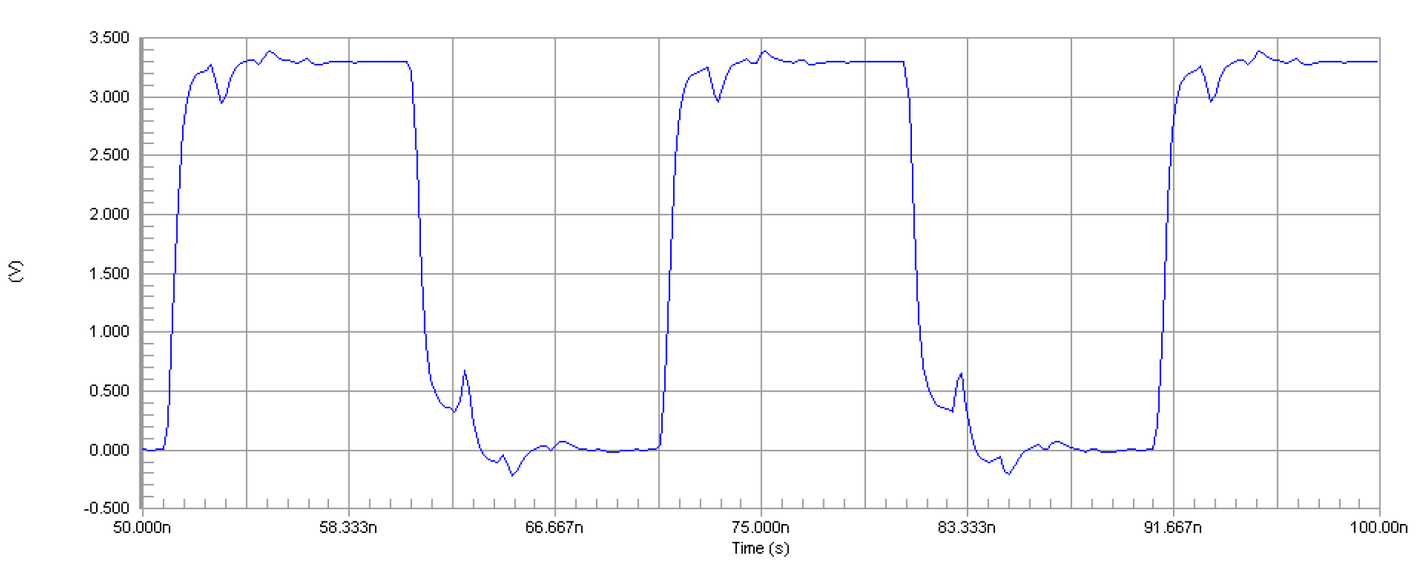
Figure 8: Altium Designer simulation waveform (at the load side) for SiT8208 driving two 5-in. transmission lines. Trace impedance – 50 Ω, supply voltage – 3.3 V, Rs = 0 Ω, CL = 5 pF.
The method of driving two transmission lines with a single source makes sure that the signals reflected from the loads interact with each other at the source in a way that they cancel out each other and no signal reflects back to the load. Signals reflected from both loads travel back to the source. At the source they reflect again and also couple through the driver into the other transmission line. If the reflection from one line is cancelled out by the coupling from the other line no signal energy is sent back to the load. For perfect cancellation the reflected signals have to reach the source at the same time and must have the same shape. The transmission lines have to be the same length and need to have balanced loads. Figure 9 shows the impact of the unbalanced capacitive load on two lines, and Figure 10 shows the impact of unmatched transmission line length.
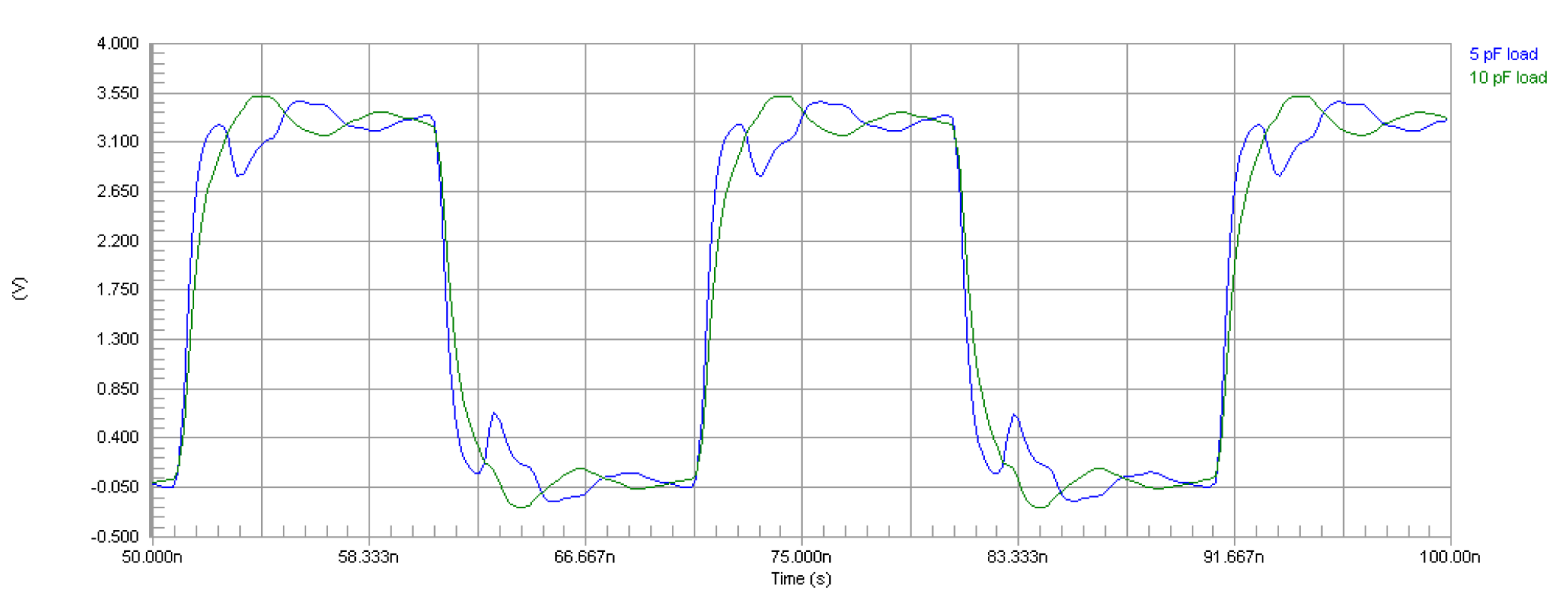
Figure 9: Altium Designer simulation waveform (at both loads) for SiT8208 driving two 5-in. transmission lines when the capacitance at the two loads is not balanced. Trace impedance – 60 Ω, supply voltage – 3.3 V, Rs = 15 Ω, CL1 = 5 pF, CL2 = 10 pF
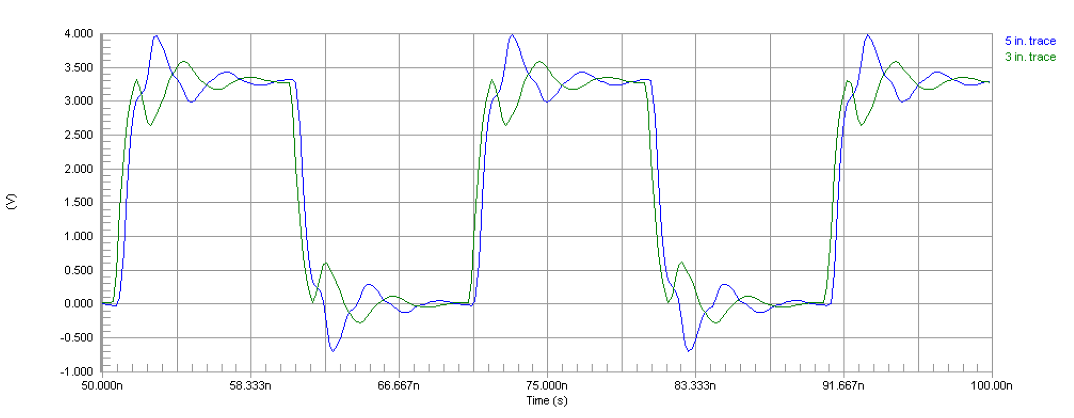
Figure 10: Altium Designer simulation waveform (at both loads) for SiT8208 driving two transmission lines of different length. Trace impedance – 60 Ω, supply voltage – 3.3 V, Rs = 15 Ω, CL = 5 pF.
3.2.3 Star topology for driving two loads
In some cases when the oscillator’s driver is not strong enough to drive two transmission lines (output impedance too high) a start topology can be used (Figure 11). The network of Rt resistors is used as a middle termination. The value of Rt is typically selected to be equal to one-third of the transmission line impedance (Z0/3), so that a star connection of three Rt resistors has an impedance of Z0/2 when looking from any node. The parallel connection of two transmission lines with Z0 impedance has Z0/2 impedance, thus when looking from point A (Figure 11) towards the load the impedance is Z0, which is equal to the impedance looking from the source. The impedance in point A is matched, so no reflection takes place there.
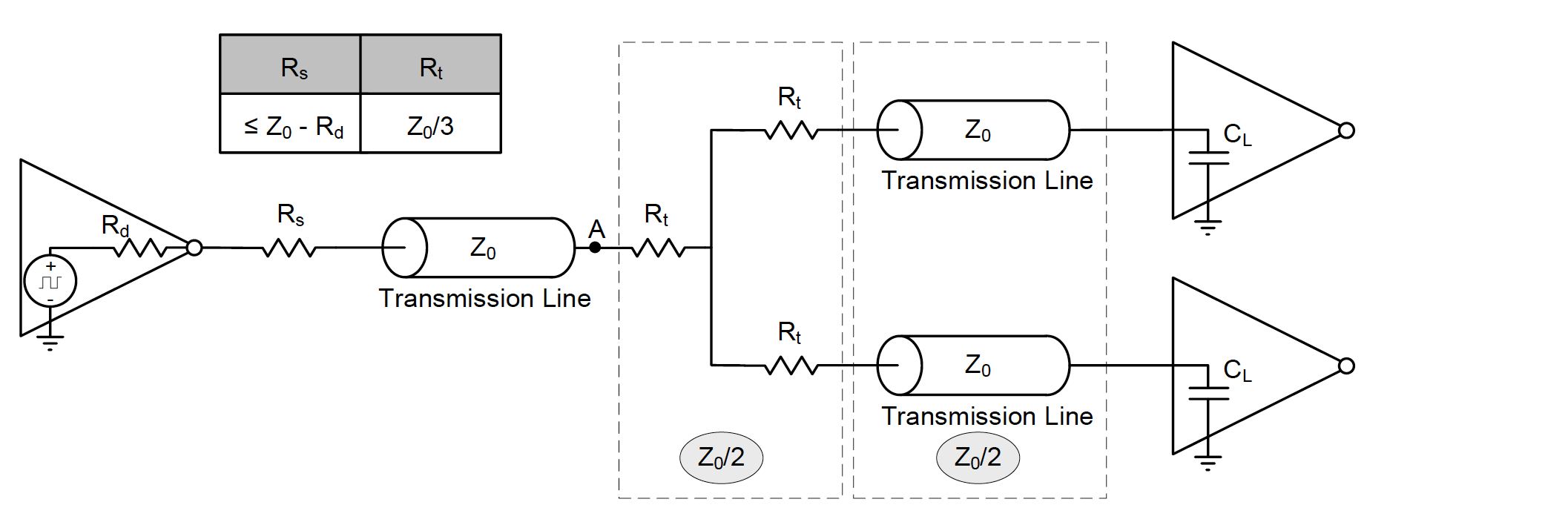
Figure 11: Star topology for driving two loads
Star topology is commonly used with the load termination. In that case signal travelling from the source driver passes trace splitting point without reflecting back, reaches the load and since the load impedance is matched doesn’t reflect back to the source. The load sees a good signal with no reflections, but very low amplitude, which is not acceptable for many clock receivers.
If there is no load termination and the load is high impedance all signal energy reflects back to the source. The impedance in the middle point is matched using Rt network, but two reflected signals are travelling back simultaneously, so the coupling occurs. It makes it very hard to find a balance between reflections and coupling and achieve acceptable signal integrity.
With no load termination this method is not recommended for use with transmission lines longer than one-third of the edge length in a trace (see Equation 1). For example, for 1 ns rise time signal the length of the star segments should not exceed 2 in. The design should be simulated using IBIS model for typical and corner cases to make sure there are no signal integrity issues. Figure 12 shows simulation results over corner cases of the star topology with short 2-in. traces.
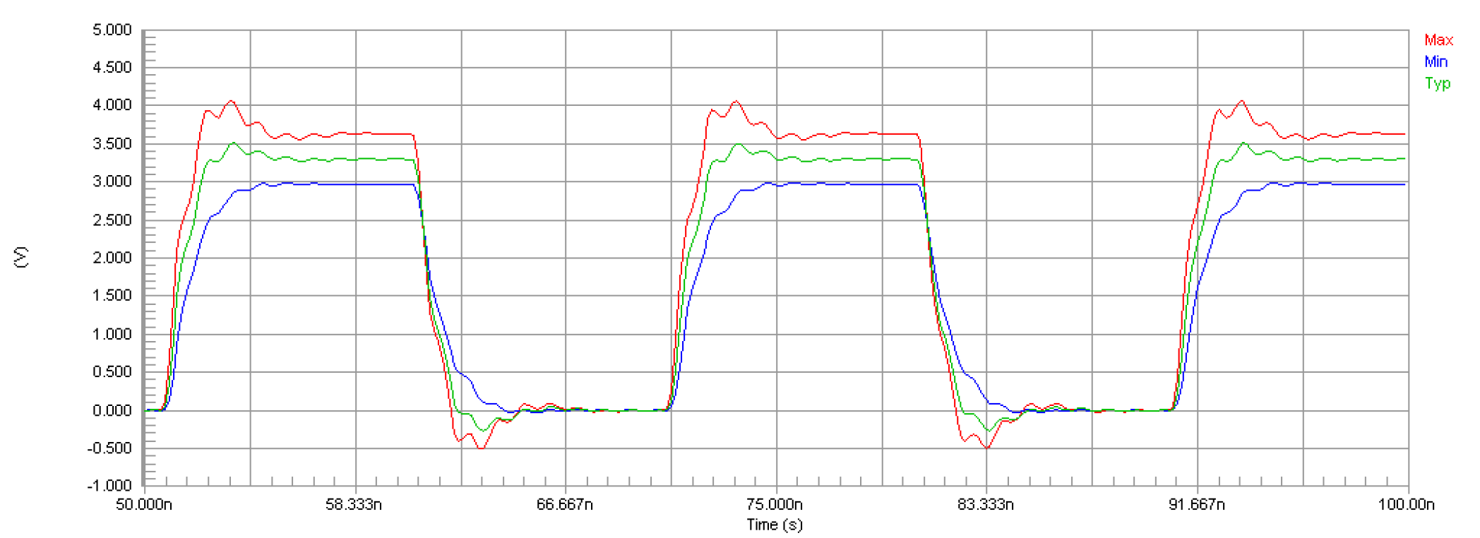
Figure 12: Altium Designer simulation waveforms (at the load side) across corners (temperature, supply voltage and process) for SiT8208 driving two transmission lines using star topology (Figure 11). Trace impedance – 60 Ω, trace segment length – 2 in., nominal supply voltage – 3.3 V, Rs = 10 Ω, Rt = 10 Ω, CL = 5 pF.
Figure 13 and Figure 14 show simulation results that illustrate how the signal waveform changes with Rt and Rs respectively.
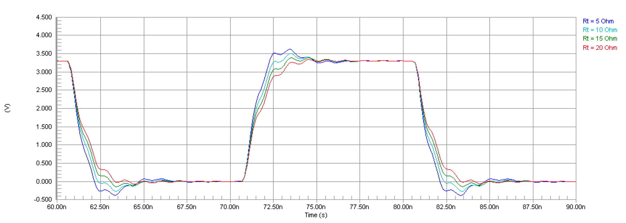
Figure 13: Altium Designer simulation waveforms (at the load side) for range of Rt values for SiT8208 driving two transmission lines using star topology (Figure 11). Trace impedance – 60 Ω, trace segment length – 2 in., supply voltage – 3.3 V, Rs = 10 Ω, CL = 5 pF.
Figure 14: Altium Designer simulation waveforms (at the load side) for range of Rs values for SiT8208 driving two transmission lines using star topology (Figure 11). Trace impedance – 60 Ω, trace segment length – 2 in., supply voltage – 3.3 V, Rt = 10 Ω, CL = 5 pF.
If there’s a need for longer traces and it is not an issue to increase signal rise/fall times then additional capacitor (Cs) may be used at the source between Rs and the transmission line, thus creating a low pass RC filter with a time constant of (Rs + Rd) x Cs. Figure 15 illustrates how using a 15 pF capacitor at the source makes it possible driving star trace topology with 5-in. segments.
Note that shapes of rising and falling edges in the examples illustrating star topology are not suitable for some jitter sensitive applications.
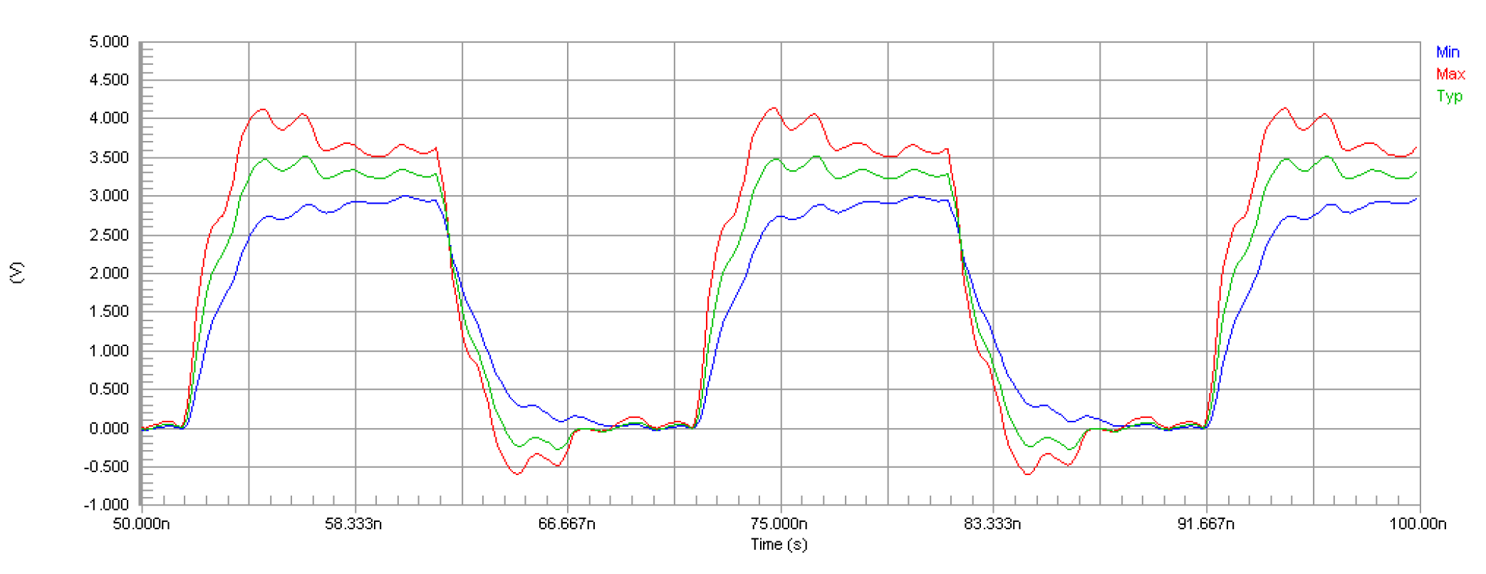
Figure 15: Altium Designer simulation waveforms (at the load side) across process corners for SiT8208 driving two transmission lines using star topology (Figure 11). Additional 15 pF capacitor at the source used to slow down signal edges. Trace impedance – 60 Ω, trace segment length – 5 in., supply voltage – 3.3 V, Rt = 10 Ω, CL = 5 pF.
3.3 Low-pass filter effect when using source termination
The signal source together with source termination drives the transmission line and sends the edge into the transmission line. At the end of the line the load doesn’t see the driver that has generated the edge, but the transmission line that has delivered it. The transmission line serves as a driver for the far-end load, so from the load perspective the drive impedance is equal to the line impedance.
The load of a clock input of a typical IC is mostly capacitive. The drive impedance is forming a low-pass filter with the load impedance which looks like a simple RC filter. The cutoff frequency of such filter is Z0CL. Assuming 50-Ω transmission line a low pass filter with a corner frequency of 637 MHz is formed.
For most applications, the corner frequency of this filter is high enough to cause no signal degradation. However, the user must monitor the load capacitance closely to ensure that the corner frequency stays comfortably above the operating range of the clock.