High Performance 2-Output, LVCMOS Automotive Clock Buffer
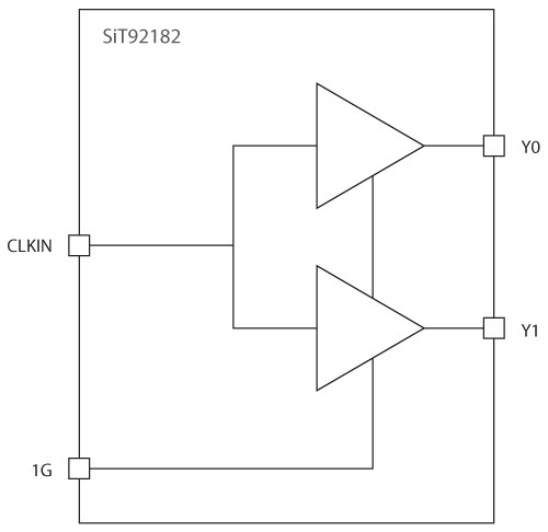
LoginThe SiT92182 is an automotive grade 1 (-40°C to 125°C), AEC-Q100-qualified, high-performance LVCMOS fanout clock buffer with low additive phase jitter of just 50 fs RMS.
This buffer supports a synchronous glitch-free output enable (OE) function to eliminate potential intermediate incorrect output clock cycles when enabling or disabling outputs. It can operate from a 1.8 V to 3.3 V supply.

Don’t waste time shipping samples. Request demo & test parts remotely in our lab and qualify for your design today.
We are ready to help you!
Please complete the form below and someone will contact you. Items notated with an * are required.
| "Specs" | "Value" |
|---|---|
| Operating Temperature Range (°C) | -40 to 125 |
| Package Type (mm²) | 2x2 mm, 8-pin DFN |
| Buffer Type | Automotive Fanout Buffer |
| Number of Inputs | 1 |
| Number of Outputs | 2 Single Ended |
| Input Type | LVCMOS |
| Input Frequency Range | 0 Hz to 200 MHz |
| Output Type | LVCMOS |
| Output Frequency Range | 0 Hz to 200 MHz |
| Additive Phase Jitter (rms) | 50 fs |
| Propagation Delay, Typical | 1.0 ns |
| Output-Output Skew, Typical | 50 ps |
| Output Enable | Yes |
| Availability | Production |
-

2x2 mm, 8-pin DFN Clock Buffer package
- High-performance 1:2 Buffer
- LVCMOS clock buffer
- Very low pin-to-pin skew: <50 ps
- Very low additive jitter: <50 fs
- Supply voltage: 1.8 V to 3.3 V
- 3.3 V tolerant input clock
- FMAX = 200 MHz
- Integrated serial termination for 50 Ω channel
- Packaged in 8 pin, 2 x 2 mm DFN packages
- AEC-Q100 qualified
- Automotive Grade 1 (-40°C to 125°C)
- Automotive Cameras
- Automotive Ethernet
- Automotive ECUs
- Automotive PCI-E
- Infotainment
- LiDAR & Radar
- Driver Monitoring Systems
- Smart Mirrors
- Engine & Powertrain
SiT92182 Evaluation Board HW User Manual – Contact SiTime
Apply Filters
| Resource Name | Resource Type | Date | Format | Size |
|---|