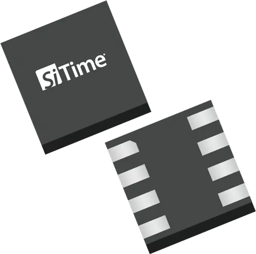
High Performance 4-Output, LVCMOS Automotive Clock Buffer
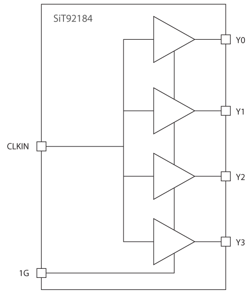
LoginThe SiT92184 is an automotive grade 1 (-40°C to 125°C), AEC-Q100-qualified, high-performance LVCMOS fanout clock buffer with low additive phase jitter of just 50 fs RMS.
This buffer supports a synchronous glitch-free output enable (OE) function to eliminate potential intermediate incorrect output clock cycles when enabling or disabling outputs. It can operate from a 1.8 V to 3.3 V supply.

| "Specs" | "Value" |
|---|---|
| Operating Temperature Range (°C) | -40 to 125 |
| Package Type (mm²) | 2x2 mm, 8-pin DFN |
| Buffer Type | Automotive Fanout Buffer |
| Number of Inputs | 1 |
| Number of Outputs | 4 Single Ended |
| Input Type | LVCMOS |
| Input Frequency Range | 0 Hz to 200 MHz |
| Output Type | LVCMOS |
| Output Frequency Range | 0 Hz to 200 MHz |
| Additive Phase Jitter (rms) | 50 fs |
| Propagation Delay, Typical | 1.0 ns |
| Output-Output Skew, Typical | 50 ps |
| Output Enable | Yes |
| Availability | Production |
-

2x2 mm, 8-pin DFN Clock Buffer package
- 3.3 V tolerant input clock
- Integrated serial termination for 50 Ω channel

- Automotive Cameras
- Automotive Ethernet
- Automotive ECUs
- Automotive PCI-E
- Infotainment
- LiDAR & Radar
- Driver Monitoring Systems
- Smart Mirrors
- Engine & Powertrain
SiT92184 Evaluation Board HW User Manual – Configure and evaluate device performance
Apply Filters
| Resource Name | Resource Type | Date | Format | Size |
|---|
