PCI Express Refclk Jitter Compliance using a Phase Noise Analyzer
DesignCon 2019, Santa Clara, CA Rohde & Schwarz Sponsored Session
January 30, 2019 Gary Giust, PhD
Disclaimers
- All opinion, judgments, and recommendations presented herein are the opinions of the presenter and do not necessarily reflect on the opinions of the PCI-SIG®.
- PCI, PCI Express, PCIe, and PCI-SIG are trademarks or registered trademarks of PCI-SIG.
- The work presented herein was conducted by Gary Giust while at JitterLabs LLC. Certain methods described herein are JitterLabs LLC patent pending
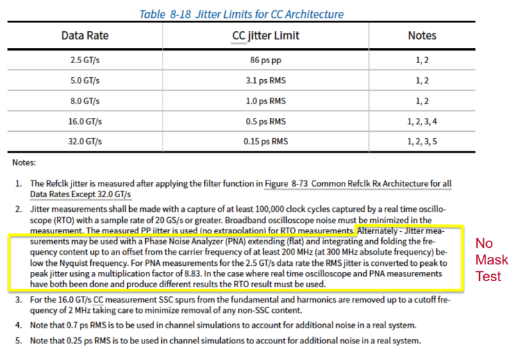
1. Motivation
PCIe4 Refclk Jitter Problem, Summary
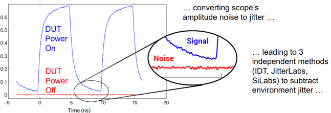
Refclk jitter can be dominated by test environment.
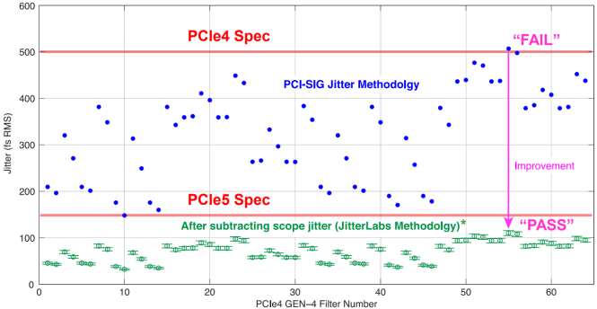
PCIe4 Refclk Jitter, Before vs After Subtracting Scope Jitter
Ultra-low noise 100 MHz HCSL clock oscillator (from DesignCon 2018 presentation).
Motivation for PCIe5 Phase Noise Method
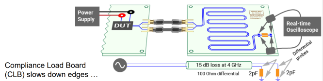
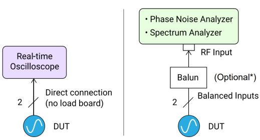
PCIe5 eliminates Compliance Load Board from refclk jitter test:
- Refclk DUT connects directly to scope
- CLB still required for testing AC, DC specifications
Interest in phase-noise based method for refclk:
- Preferred by clock/timing industry (easier, faster, lower noise floor)
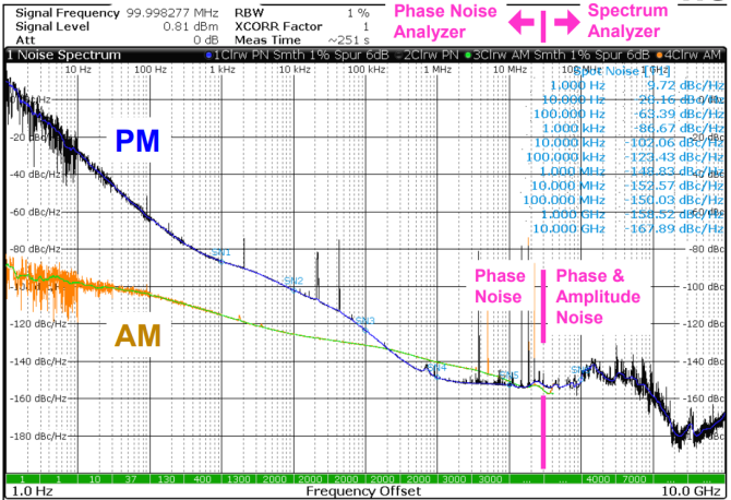
- But, oscilloscope, phase noise analyzer, spectrum analyzer observe jitter differently
- Led to creation of new, alternative, normative specification based on phase noise analyzer (not spectrum analyzer) data *
- Scalable for future PCIe generations
- Oscilloscope refclk jitter test remains (needed for in-system measurements)
* Goal is to create a methodology to derive jitter from phase noise that results in same jitter as derived from oscilloscope using traditional PCISIG methodology
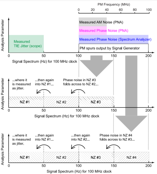
2. How Phase Noise Aliases in Sampled Systems
Input Jitter Aliases when Sampled by PLL
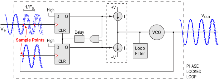
- Let FS = sample rate of phase detector
- An input jitter frequency above FS / 2 will alias below FS / 2 when sampled
- The aliased jitter frequency is then filtered by the PLL jitter transfer function
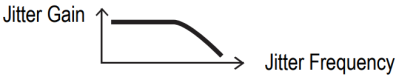
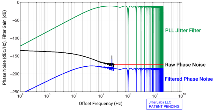
Example PLL Jitter Transfer Function
Modeling Phase Noise Aliasing through PLL
Alternate (equivalent) Model Accounting for Phase Noise Aliasing through PLL
Jitter vs PN Aliasing
Article: Phase Noise Aliases as Jitter
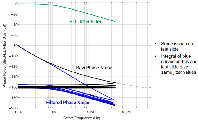
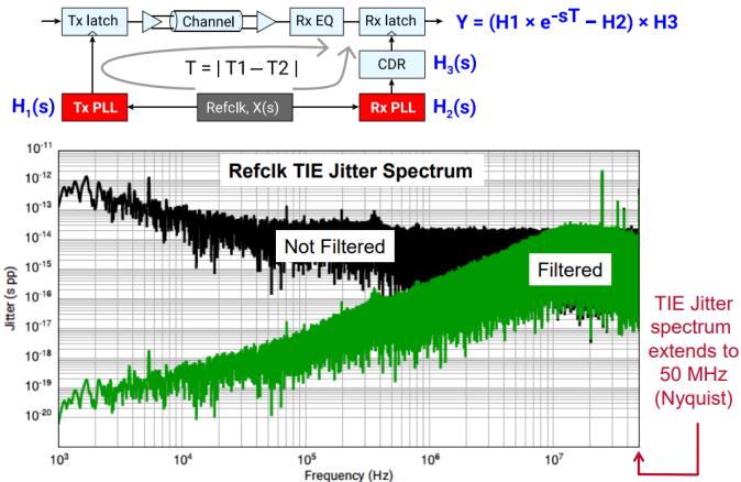
Jitter Filtering from Common Clock Architecture (example)
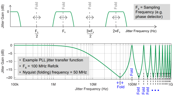
Conventional Derivation of Jitter from Phase Noise (does not account for aliasing)
- Extend phase noise data to 50 MHz
- Compute jitter filter to 50 MHz
- Filter phase noise
- Integrate filtered phase noise to compute jitter
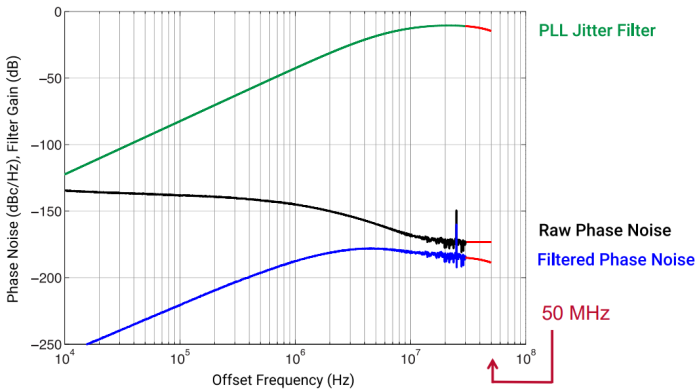
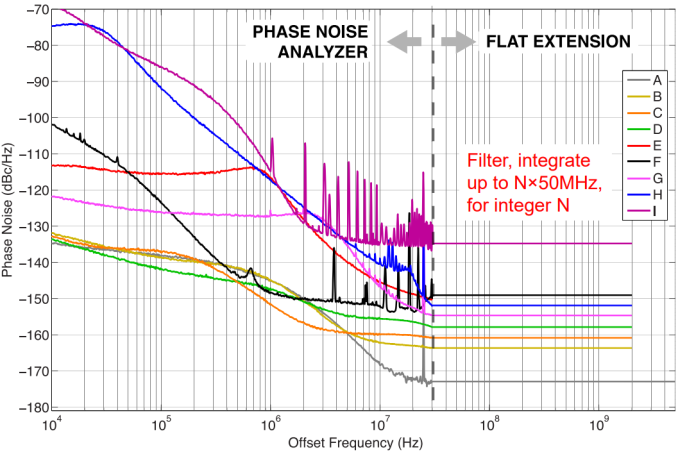
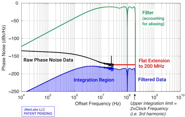
Recommended Derivation of Jitter from Phase Noise (accounts for aliasing)
- Extend phase noise data to ? MHz
- Compute jitter filter to 50 MHz, mirror it across N×FS /2 spectral boundaries (N=integer)
- Filter phase noise
- Integrate filtered phase noise to compute jitter
3. Algorithm Development: Test Setup and Results
PCIe GEN-5 (32GT/s) Refclk Jitter Test Setup
* Article: Measuring Phase Noise with Baluns
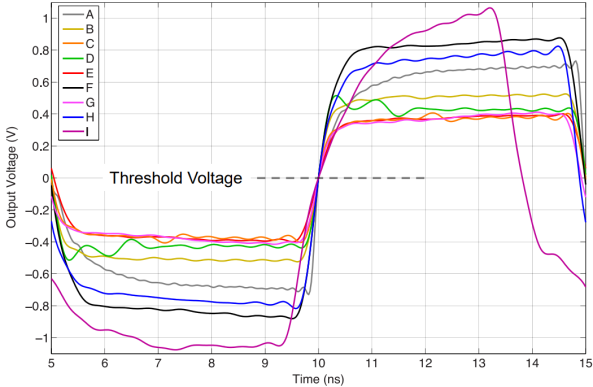
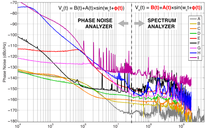
Analyzed 9 Clocks from 4 Manufacturers, Signal Integrity
Example FSWP Acquisition, DUT #1
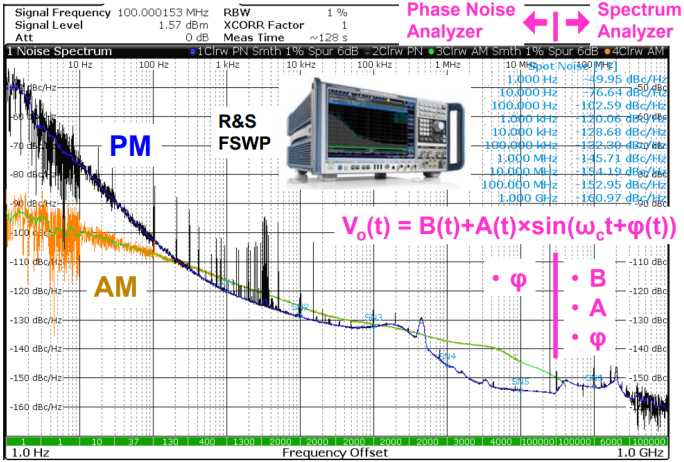
Example FSWP Acquisition, DUT #2
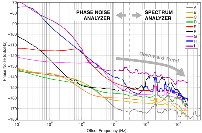
Raw Phase Noise (9 clocks from 4 mfgrs)
Article: Influence of Noise Processes on Jitter and Phase Noise Measurements
Phase Noise with Spurs Omitted, 1% Smoothing
Phase Noise with Appended Extensions
4. Algorithm Development: Data Analysis
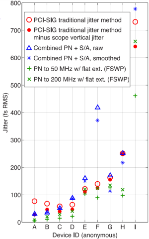
Jitter Results
- 16 unique jitter filters for 32GT/s
- Analyze 1 filter for all devices (highest jitter)
Device G Analysis (similar to A-E, I)
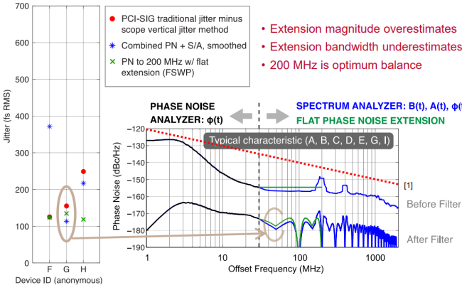
[1] Determine the Dominant Source of Phase Noise
Outlier Device F: Spectrum Analyzer Assumes Wrong
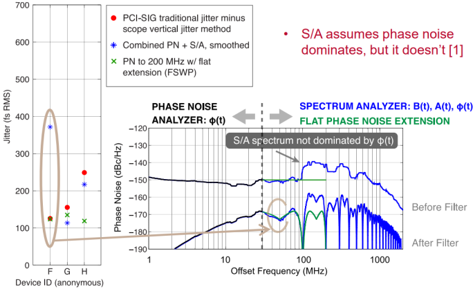
[1] Influence of Noise Processes on Jitter and Phase Noise Measurements
Outlier Device H: Excessive Near-in Phase Noise
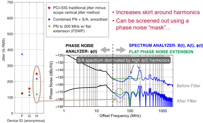
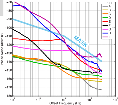
Phase Noise “Mask” Test
- Measure phase noise
- Omit spurs (or smooth)
- Evaluate against mask
- Eliminates devices with excessive near-in phase noise, which have high harmonic content,
- which improves matching between scope and phase noise methods.
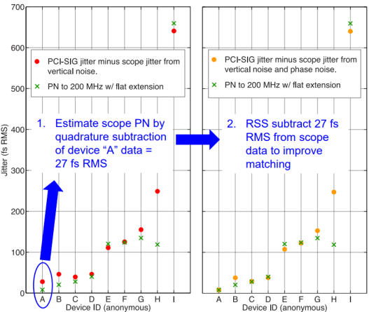
Subtract Scope-timebase Phase Noise
5. Recommended Phase Noise Methodology
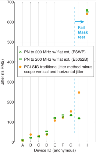
Final Comparison
- Add E5052B data
- Shows good agreement
PCIe5 32 GT/s Common Refclk Model
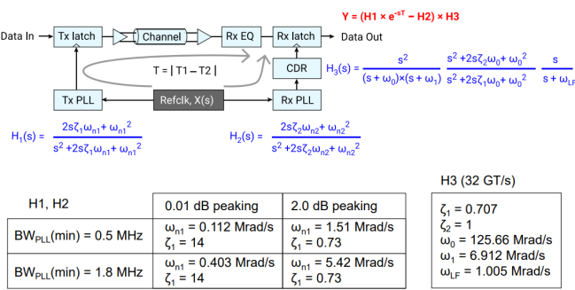
Source: PCI Express Revision 5.0, Version 0.9, www.pcisig.com
Adopted into PCIe5 Refclk Jitter Spec
Source: PCI Express Revision 5.0, Version 0.9, www.pcisig.com
Summary of PCIe5 Jitter Compliance via Phase Noise
Independent Verification from Data Converter Industry
While theory [1] states to integrate phase noise up to clock-input bandwidth, empirical results comparing phase jitter derived from SNR measurements
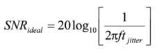
with that from integrating phase noise with flat extensions show good agreement when upper offset frequency for integration equals twice the carrier frequency. This approach is common in the literature [2,3] dating at least back to 2008.
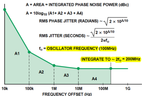
Calculating jitter from phase noise
[1] “Sampled Systems and the Effects of Clock Phase Noise and Jitter” B. Brannon, app note AN-756, Analog Devices, (2004).
[2] “Analog-to-Digital Converter Clock Optimization, a Test Engineering Perspective” R. Reeder, W. Green, R. Shillito, Analog Dialogue, 42-02, Analog Devices (Feb. 2008).
[3] “Interfacing to Data Converters” section 6.5 (Sampling Cock Generation), W. Kester, Analog Devices.
6. Conclusion
1. Phase noise aliases in sampled systems
2. New method to estimate scope jitter by
- Extending phase noise up to twice the clock frequency (e.g. 200 MHz offset)
- Filtering, accounting for aliasing
- Integrating to convert to jitter
3. Refclk jitter in PCIe Base Spec Revision 5.0 Version 0.9 (10/18/2018)
- Oscilloscope-based method continues
- Requires compliance load board GEN 1 to 4, but not GEN 5
- Alternate, normative, phase-noise based method is fast, easy
- Can be used for GEN 1 to 5, no compliance load board
- Requires phase noise analyzer (spectrum analyzer not allowed)
- If data collected for both scope and phase noise methods, then scope data must be used
Contact SiTime for Clock & Timing Solutions