Power Supply Noise Rejection and Layout Considerations for SiT9514x Devices
Content
1. Introduction
2. Power Supply Considerations
2.1 Switching versus Linear Supplies
2.2 Overview and PSNR Measurement Methodology
3. Power Supply Noise Performance
3.1 PLL VDD Supply @ 3.3V
3.2 PLL VDD @ 2.5V
3.3 Output Driver Supply VDDO
3.4 PLL Phase Noise Plots with 10-mV Peak to Peak Ripple on the Supply
4. Power Supply Related: Best PCB Design and Layout Guidelines
5. Cross Talk Reduction and Signal Integrity: Best Layout Practices for Signal Lines
6. Thermal Noise Reduction: Best Layout Practices
1. Introduction
The SiT95141, SiT95143, SiT95145, SiT95147, and SiT95148 network synchronizers, jitter cleaners / attenuators, and clock generators are highly resistant to shock, vibration, and power-supply noise, making them ideally suited for robust performance in the field. This document provides information about the power supply noise rejection (PSNR) performance of the SiT9514x products. Also provided are layout guidelines and best practices for customers using the SiT9514x parts in their design.
2. Power Supply Considerations
This section discusses the background of power supply noise, PSNR performance measurement methodologies, and measurement data for the SiT9514x parts with respect to PSNR performance.
2.1 Switching versus Linear Supplies
There are two alternate ways to regulate the incoming line supply down to the voltage needed for the various supplies of the SiT9514x chip. The first option is to use a linear low drop out (LDO) regulator and the second option is to use a switching DC-DC converter.
Linear LDOs do not have switching noise at the output; they have relatively better noise performance and are usually easier to design on the board. Therefore LDOs are recommended for all supplies of the SiT9514x device for best noise performance. However, for applications where overall power efficiency is of paramount concern, an LDO may not always be the best solution. This is because the “drop out” of voltage from the input voltage to the output regulated voltage appears across the output power transistor commonly known as the “pass transistor.” This causes a loss of efficiency due to dissipation of energy across the pass transistor which appears as a resistive element.
This efficiency loss can be avoided by using switching DC-DC converters that use inductors and capacitors as storage elements in the control loop to perform regulation. For example energy might be periodically stored and released from the magnetic field in an inductor into the electric field of a capacitor at a rate that is determined by a control loop to maintain the required output voltage regulation. However since this causes switching noise at the output, the output-regulated voltage from the DC-DC converter is not as clean.
This trade-off between the performance advantage of an LDO and the efficiency advantage of a switching DC-DC converter is usually resolved by system designers by using various combinations of these voltage converters. For example, a switching DC-DC converter might be used to down convert from a high voltage supply to an intermediate supply, that is then down converted to the desired output voltage by an LDO.
2.2 Overview and PSNR Measurement Methodology
SiT9514x products have excellent PSNR performance. As described in the previous sub-section, there are several options for designing the supply architecture using a combination of LDOs and switching DC-DC converters. Therefore to obtain a quantitative understanding of the PSNR performance, a clean and comprehensive methodology is required.
A wide bandwidth bias-tee is used to provide a sinusoidal ripple as the noise source superimposed on the DC supply voltage. This sinusoidal ripple is applied directly to the VDDO supply pin on the device with all decoupling capacitors removed. It is important to remove all decoupling capacitors on the supply being characterized while making the PSNR test measurement. This is to ensure that the exact waveform of the sinusoid superimposed on the DC voltage is actually incident on the device’s supply pin. In addition the device supply pin is monitored on an oscilloscope. The block diagram showing the test setup is shown in Figure 1.
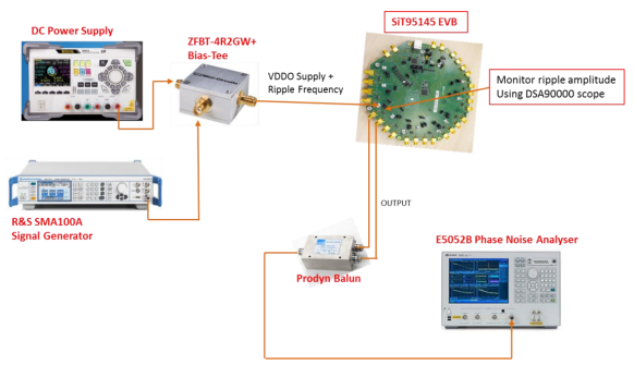
Figure 1. Block diagram of the PSNR test setup
The PSNR for the VDD (PLL) supply as well as the VDDO (output driver) supply are considered separately. The PSNR performance from the VDDIN supply is significantly superior to the VDD supply.
Based on this test, the RMS integrated jitter for various levels of ripple is computed. Note that the PSNR data used for this analysis is with the supply decoupling capacitor completely removed from the PCB.
This performance could improve with supply decoupling capacitors and filtering chokes which are already present on the EVB and are recommended to be used on the customer boards.
The PSNR is measured with a sine wave ripple added in series with the supply. Under this condition the relative dBc spur in the output is measured in the output phase noise plot.
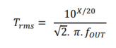
A spur in the output at X dBc relative to the carrier at an output frequency of f_OUT can be expressed in terms of RMS jitter as per the following calculation:
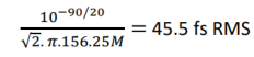
For example, a -90 dBc output spur relative to carrier at 156.25 MHz output results in an RMS jitter addition of
For example, phase jitter (with no spur) of 150 fs will translate to a jitter of
3. Power Supply Noise Performance
3.1 PLL VDD Supply @ 3.3V
Table 1. PLL VDD Supply @ 3.3V
Overall total jitter (assuming native jitter of 150 fs RMS) is shown with the ripple on the supply.
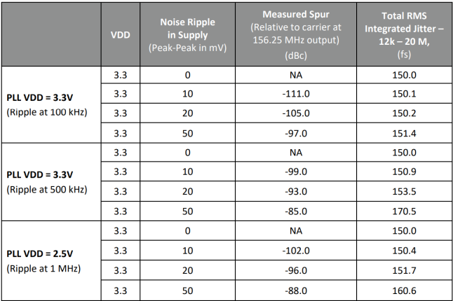
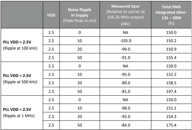
3.2 PLL VDD @ 2.5V
Table 2. PLL VDD @ 2.5V
Overall total jitter (assuming native phase jitter of 150 fs RMS) is shown with the ripple on the supply.
3.3 Output Driver Supply VDDO
Table 3. LVPECL; Spurs (dBc) measured on E5052B Phase Noise Analyzer
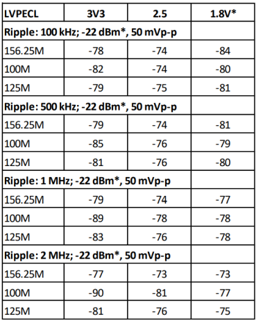
*Note that LVPECL VDDO is supported down to 2.5V, whereas LVPECL2 VDDO is supported down to 1.8V
Table 4: LVDS; Spurs (dBc) measured on E5052B Phase Noise Analyzer
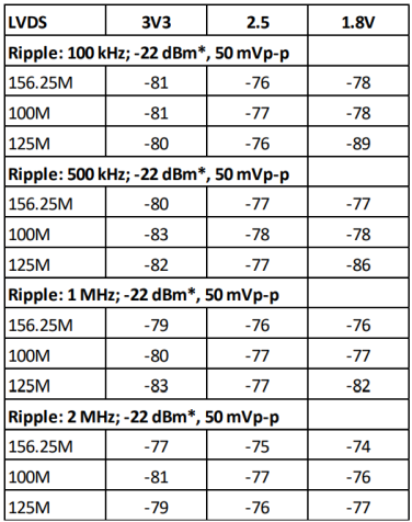
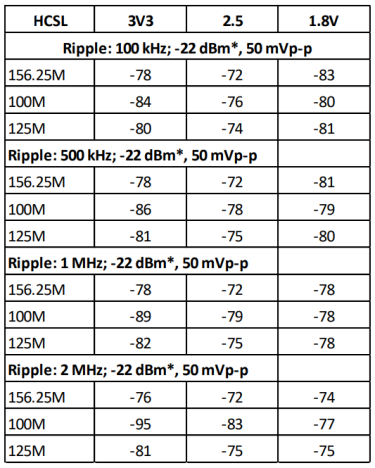
Table 5: HCSL; Spurs (dBc) measured on E5052B Phase Noise Analyzer
3.4 PLL Phase Noise Plots with 10-mV Peak to Peak Ripple on the Supply
The previous section shows the jitter degradation with a noise ripple added in series with the supply. The output spurious components at various frequency offsets are measured as a relative dBc spur. This is the comparison metric that is usually used in datasheets. Additionally, phase noise plots are taken with a 10-mV peak to peak ripple on the supply at 100k and 1M offset frequencies. 100k and 1M represents the usual range of frequencies expected from a switching power supply. A 10-mV peak to peak represents a worst case ripple on a moderately filtered switching supply.
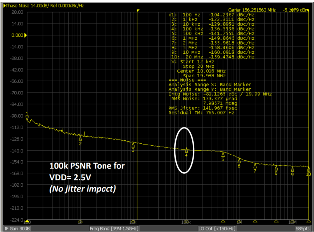
Figure 2. SiT9514x (VDD= 2.5 V, fspur = 100 kHz, Vspur= 10 mV pp)
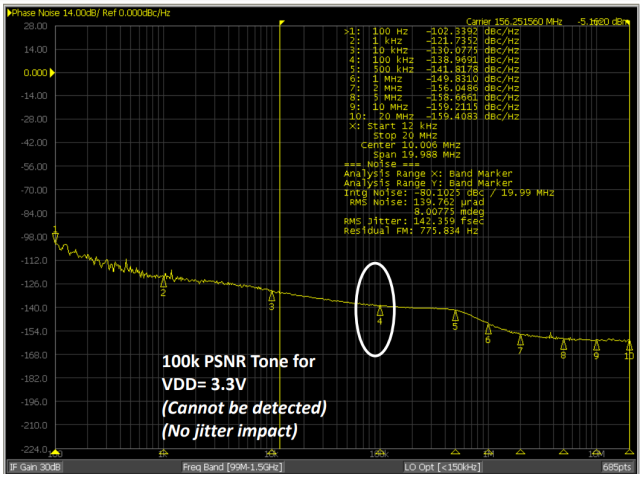
Figure 3. SiT9514x (VDD= 3.3V, fspur = 100 kHz, Vspur= 10 mV pp)
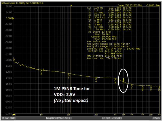
Figure 4. SiT9514x (VDD= 2.5V, fspur = 1 MHz, Vspur= 10 mV pp)
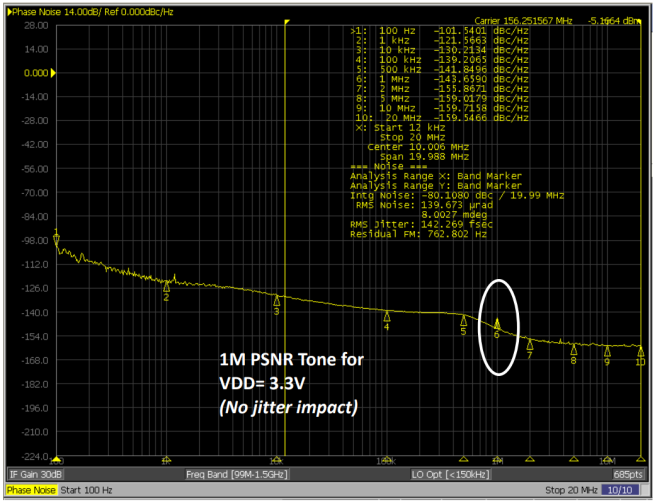
Figure 5. SiT9514x (VDD= 3.3 V, fspur = 1 MHz, Vspur= 10 mV pp)
4. Power Supply Related: Best PCB Design and Layout Guidelines
Power supply noise is rejected to the extent of the PSNR provided by the chip by way of integrating LDOs inside the chip. This is a finite amount of rejection that is provided by the chip and is discussed in the previous section of this document. The power supply that is provided to the chip on the main PCB should follow these guidelines to provide the cleanest supply possible to the clock chip.
Decoupling caps with low ESR should be placed next to every supply pin on the clock chip. This provides a charge storage and also provides filtering.
- For the best noise performance, provide a dedicated LDO that supplies to the clock chip on the main system to avoid cross talk to any other system through the common LDO.
- If dedicated LDOs can’t be provided, then provide a separate LC filter to each supply of the clock chip so that the noise / disturbance at the common LDO output can be filtered.
- Ensure that the VDD and GND planes are running next to each other so that any external high frequency current loops between supply and ground are well contained.
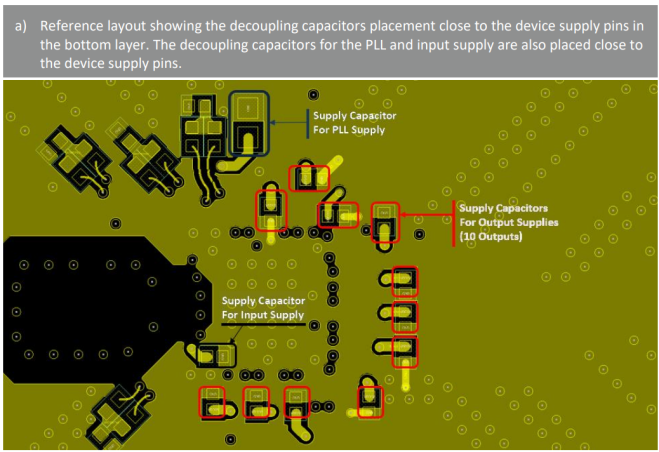
Figure 6. Supply decoupling capacitors
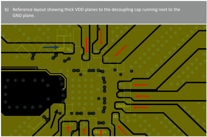
Figure 7. VDD routing illustration
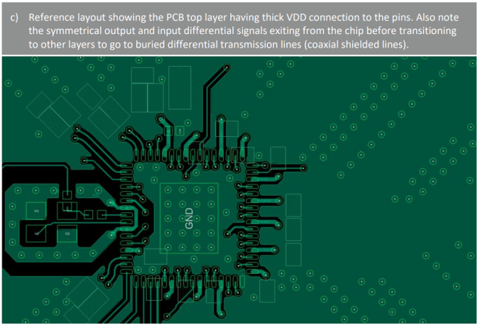
Figure 8. Top layer VDD connections to the pins
5. Cross Talk Reduction and Signal Integrity: Best Layout Practices for Signal Lines
Care needs to be taken to avoid coupling (capacitive and/or inductive) between adjacent channel (input and output differential pair) traces. Capacitive coupling usually results when one trace lies on top of another trace. This coupling is a direct function of the distance between the trace and an overlap area. This coupling may be so severe that parallel channels should be avoided at all times. Inductive coupling involves traces that are physically located in close proximity to each other. With two traces adjacent to each other, current flowing down one of the traces (aggressor) will couple into the adjacent trace (victim).
Spatial proximity should therefore always be avoided for critical signals.
- Make sure the distance between critical signal paths is maximized to minimize the crosstalk between the two differential pairs.
- Keep the length of the two differential traces the same to minimize the skew and phase difference.
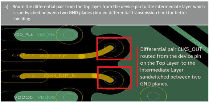
Figure 9. Signal exit near the chip pins
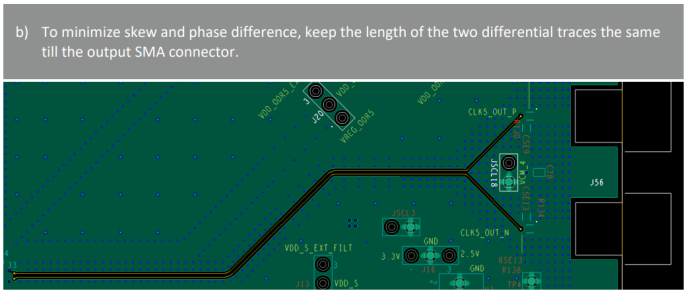
Figure 10. Matched routing of the differential lines
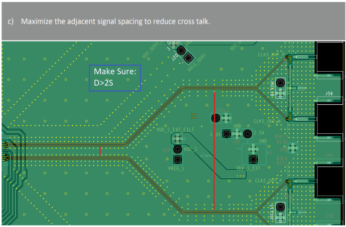
Figure 1. Critical signals should be spaced far apart for cross talk reduction
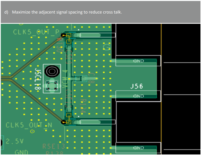
Figure 2. Output termination and SMA connection
6. Thermal Noise Reduction: Best Layout Practices
The QFN package is designed so that the lead frame die pad (or thermal pad) is exposed on the bottom of the IC. This provides an extremely low thermal resistance (θJA) path between the die and the exterior of the package.
The solder-mask-defined thermal pad is the exposed copper area not covered by solder mask. It must be soldered directly to the thermal pad on the bottom of the IC.
It is recommended to place thermal vias in the solder-mask-defined thermal pad to effectively transfer the heat from top copper layer of the PCB to the inner or bottom copper layers. The thermal vias should make their connection to the internal ground plane with a complete connection around the entire circumference of the plated through hole.
Figures 13 and 14 show a reference layout of the thermal PAD on the top layer and bottom layer which connects to the device thermal ePad.
Figure 3. Top Layer
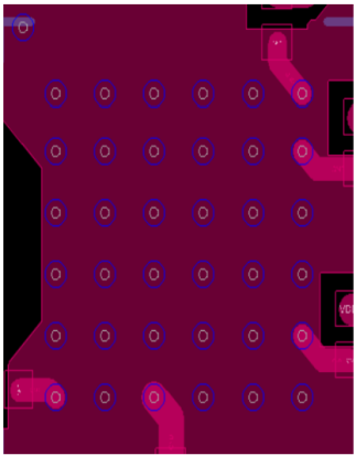
Figure 4. Bottom Layer
Inner or bottom-layer copper planes can also be connected to the thermal ePad by using vias and should be made as large as possible. The thermal pad is usually tied to ground, and designers should ensure electrical correctness when connecting the copper planes to the thermal pad. The bottom copper plane may be left exposed for improved thermal performance.