Content
2.1 Termination Recommendations for DC-Coupled Applications
2.2 Termination Recommendations for AC-Coupled Applications
3.1 Termination Recommendations for DC-Coupled Applications
3.2 Termination Recommendations for AC-Coupled Applications
5 Driving HCSL Receiver with LVPECL Oscillators
Driving CML Receiver with LVPECL Oscillators
7 Driving Self-Biased Differential Inputs
8 Driving an LVDS Receiver with an LVPECL Driver
9 Interfacing an LVCMOS Oscillator into an LVDS/LVPECL Input
Additional Content in the PDF:
Appendix A: Transmission Line Termination Impedance Matching
A.1 Load Termination
A.2 Source Termination
A.3 Double Termination
1. Introduction
Differential oscillators are used in high performance applications and offer several benefits such as higher robustness to power supply noise. This application note provides termination recommendations for the SiTime differential oscillator families listed in Table 1, with LVPECL, LVDS, or HCSL output drivers. Interfaces for driving CML or HCSL clock inputs with LVPECL output are also discussed.
Typical output rise and fall times of SiTime oscillators are in range of 250 ps to 600 ps, which causes even short traces on a PCB to behave like distributed transmission lines that require impedance matching. Therefore, it is recommended to design traces for differential signals as controlled impedance transmission lines with matched length. Those traces should be terminated properly for best signal integrity and lowest EMI. In addition to impedance matching, termination networks also impact DC bias and AC voltage swing at the receiver side.
Table 1: SiTime Differential Oscillators
|
Device Family |
Oscillator Type |
Output Driver Types |
|
Differential Oscillators |
LVPECL, LVDS |
|
|
Differential Oscillators |
LVPECL, LVDS |
|
|
Differential Oscillators |
LVPECL, LVDS |
|
|
SiT9365 |
High-Performance Differential Oscillators |
LVPECL, LVDS, HCSL |
|
High-Performance Differential Oscillators |
LVPECL, LVDS, HCSL |
|
|
High-Performance Differential Oscillators |
LVPECL, LVDS, HCSL |
|
|
High-Performance Differential Oscillators for Automotive |
LVPECL, LVDS, HCSL |
|
|
High-Performance Differential Oscillators for Automotive |
LVPECL, LVDS, HCSL |
|
|
Voltage Controlled Oscillators (VCXO) with DE |
LVPECL, LVDS |
|
|
SiT3822 |
Voltage Controlled Oscillator (VCXO) with DE |
LVPECL, LVDS |
|
High-Performance Voltage Controlled Oscillators (VCXO) with DE |
LVPECL, LVDS, HCSL |
|
|
High-Performance Voltage Controlled Oscillators (VCXO) with DE |
LVPECL, LVDS, HCSL |
|
|
Voltage Controlled Oscillators (VCXO) with DE |
LVPECL, LVDS |
|
|
Voltage Controlled Oscillators (VCXO) with DE |
LVPECL, LVDS |
|
|
High-Performance Spread-Spectrum Oscillators (SSXO) with DE |
LVPECL, LVDS, HCSL, CML |
|
|
High-Performance Digitally Controlled Oscillators (DCXO) with DE |
LVPECL, LVDS, HCSL |
|
|
High-Performance Digitally Controlled Oscillators (DCXO) with DE |
LVPECL, LVDS, HCSL |
|
|
Temperature Controlled Oscillators (TCXO) with DE |
LVPECL, LVDS |
|
|
Temperature Controlled Oscillators (TCXO) with DE |
|
2. LVPECL Output
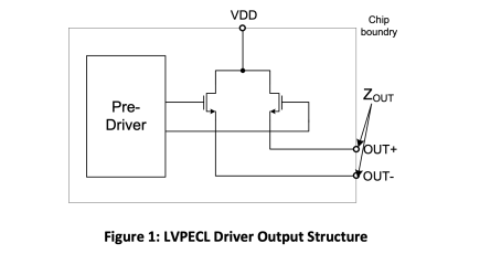
Figure 1 shows a low-impedance LVPECL driver structure that is used in SiTime differential oscillator families. An output stage of a driver consists of a pair of NMOS transistors in common source configuration. Typical driver impedance is about 5Ω to 10Ω.
2.1 Termination Recommendations for DC-Coupled Applications
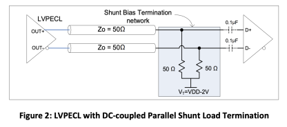
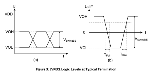
LVPECL is typically terminated at the load side, as shown in Figure 2. Outputs are connected to a termination voltage (VT) with 50Ω resistors, providing good impedance match to the transmission line (See Appendix A for load termination analysis). Figure 3(a) illustrates a single-ended waveform of the LVPECL output with typical termination. The typical voltage output high (VOH) and voltage output low (VOL) signal levels are VDD – 0.9V and VDD – 1.7V, respectively. VOH and VOL limits specified in the datasheet take into account output driver impedance variation from part to part and external load conditions.
The voltage swing of the differential waveform between positive and negative outputs (VDiff = VOUT+ -VOUT-) is twice as much as the single-ended signal voltage amplitude. Typical LVPECL differential swing is 1.6V. Figure 3(b) illustrates how 20% to 80% rise and fall times are defined for a differential waveform.
Note that VOH, VOL, and voltage swing depend on termination and can be different if non-default termination is used.
If an LVPECL receiver does not have a built-in termination, external 50Ω termination resistors should be placed as close as possible to the receiver to reduce un-terminated stubs that can cause signal integrity issues. A transmission line should be terminated at the load side only.
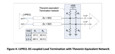
In applications where a separate termination voltage is not readily available, pull-up and pull-down resistors forming a Thevenin Equivalent network can be used to terminate 50Ω transmission lines (see Figure 4). Such a network establishes DC bias voltage of VDD – 2V at receiver inputs and effective 50Ω termination impedance. Note that the resistor values are different for 3.3V and 2.5V supply voltages.
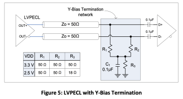
In most cases Thevenin Equivalent termination works well, but it can be sensitive to power supply noise if there is any significant mismatch between traces or between resistor networks on each side of the differential pair, or if the receiver is too sensitive to common-mode noise. Figure 5 shows the Y-Bias termination network, which provides an effective termination voltage of VDD – 2V without requiring either connection to VDD or access to an additional termination voltage source. The termination voltage is generated by the sum of differential pair currents passing through resistor R3. The capacitor C1 is used to create AC ground at the termination voltage.
2.2 Termination Recommendations for AC-Coupled Applications
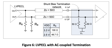
An LVPECL receiver may be either DC- or AC-coupled. AC-coupling capacitors are required if DC bias voltages at the receiver and oscillator sides are different. In some cases a termination network has to be AC-coupled, as shown in Figure 6. For proper LVPECL driver operation, its output transistors should never be completely turned off, so additional bias resistors RB, placed before AC-coupling capacitors, are required to provide a DC current path for the driver. The value of RB is selected such that the minimum current through a driver pin when the pin is in low state is not less than 3 mA, and maximum DC current through a driver does not exceed 30 mA. Equation 1 can be used to estimate RB.
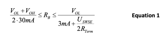
In Equation 1, USWSE is single-ended voltage swing and RTerm is termination network resistance. SiTime recommends using RB values of 100Ω and 48.7Ω for 3.3V and 2.5V supply respectively.
The following recommendations should be followed to achieve best signal integrity with LVPECL parallel load terminations:
1. Place the termination network within 0.1 to 0.2 inches from the receiver. Long traces connecting the termination network to the receiver appear as stubs and can degrade signal integrity at the receiver inputs.
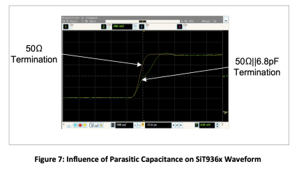
2. Minimize capacitive loads at the receiver input. High capacitive loads reduce termination impedance when fast signal edges reach the receiver, causing a large load reflection coefficient. This reflection returns to the load with a little attenuation after being reflected at the source. The rule of thumb is that the termination mismatch becomes significant if 3Tr / (Pi x Cl) < 50 Omega, where Tr is the 20% to 80% rise time, and CL is the load capacitance. Figure 7 shows an example of how 6.8 pF of parasitic input capacitance affects the rising edge of the LVPECL waveform.
3 LVDS Output
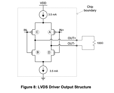
LVDS is a high-speed digital interface suitable for many applications that require low power consumption and high noise immunity. LVDS outputs use differential signals with low voltage swings to transmit data at high rates. Figure 8 shows the output structure of an LVDS driver, consisting of 3.5 mA nominal current sources connected to differential outputs via a switching network, sometimes referred to as “H” switch. The outputs are typically connected to 100Ω differential transmission lines terminated with a 100Ω resistor across the receiver inputs. The resistor value matches the impedance of the transmission lines and provides a current path for the signal.
The driver includes circuitry to set the common mode to 1.2 V nominally regardless of VDD. Therefore, there is no need for externally biasing the driver to any specific voltage. Also, an LVDS output can be connected to any LVDS input without any concern for the actual supply voltage of the oscillator.
Signal switching is accomplished with four transistors labeled A, B, C, and D. Since the impedance of the receiver is typically high, virtually all current from the driver flows through the 100Ω resistor, resulting in a voltage difference of 350 mV between the receiver inputs. In Figure 8, when the signal IN is low, transistors A and B are turned on; the current flows through transistor A and the 100Ω resistor, and returns through transistor B. When the signal IN is high, transistors C and D are turned on; the current flows through transistor C and the 100Ω resistor, and returns through the transistor D, resulting in -350mV voltage across the receiver.
From the receiver standpoint, the direction of the current flowing through the termination resistor determines whether a positive or negative differential voltage is registered. A positive differential voltage represents a logic high level, while a negative differential voltage represents a logic low level.
3.1 Termination Recommendations for DC-Coupled Applications
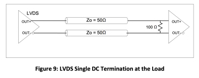
An LVDS interface with 100Ω differential traces is typically terminated at the receiver end with a 100Ω resistor across the differential inputs of the receiver (see Figure 9). Some receivers incorporate a 100Ω on-chip resistor, eliminating the need for external termination.
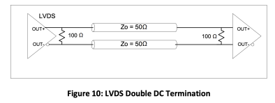
For most applications, a single termination at the load is sufficient. In situations where the load reflection coefficient is relatively high, a double termination arrangement may reduce the overall round trip (see Figure 10). With a 100Ω resistor at both the source and the load, the equivalent resistance at the output driver is reduced to 50Ω, causing the output signal swing to be cut in half.
Appendix A: Transmission Line Termination Impedance Matching has more information on the uses of single and double termination arrangements.
3.2 Termination Recommendations for AC-Coupled Applications
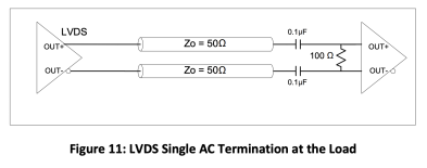
If an LVDS driver and receiver are operating with different common mode voltages, an AC termination is recommended. A capacitor is used to block the DC current path from the driver, so the receiver must implement its own input bias circuit.
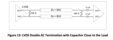
AC coupling can be configured as either a single termination at the load, or as a double termination. Single termination is shown at Figure 11. For both single and double terminations, AC-coupling capacitors can be placed before (shown in Figure 12) or after (shown in Figure 13) the load termination resistor.
The double terminations shown in (Figure 12 and Figure 13) differ only in the position of the AC-coupling capacitor. The capacitor in Figure 12 is charged by the common mode current flowing through half the differential resistance, which is the equivalent of 50Ω. The capacitor in Figure 13 is charged by the current through the resistance of the receiver inputs, which can be in the range of several tens of kiloohms. During clock startup, the capacitor shown in Figure 12 is charged much faster than that shown in Figure 13. Therefore, a valid clock signal will be available to the receiver sooner. If fast clock startup is important, the configuration shown in Figure 12 is preferable.
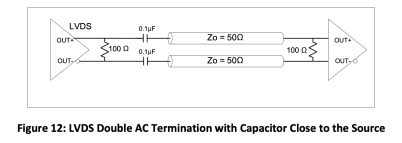
In data transmission applications, the configuration shown in Figure 13 may be more advantageous. Because of its higher RC time constant, it can sustain data sequences with longer 1s and 0s without experiencing significant voltage droop.
4. HCSL Output
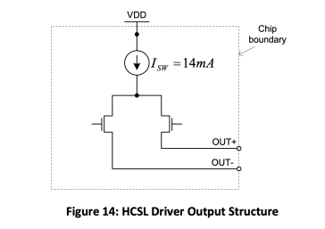
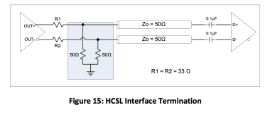
The HCSL driver option is available only in some SiTime oscillator families. The HCSL output structure (see Figure 16Figure 14) is driven by a 14 mA switched current source typically terminated to ground via a 50Ω resistor as shown Figure 15. The nominal signal swing is 700 mV. The open-drain transistor at the output has fairly high impedance in the range of several kilo-ohms. From an AC standpoint, the output transistor impedance is parallel to the 50Ω load resistor, resulting in an equivalent resistance very close to 50Ω. Since the traces used in this interface have a characteristic impedance of 50Ω, any signal reflected from the load will be absorbed at the source. Typically two small resistors, R1 and R2 (see Figure 15), are placed in series with the high-impedance driver. They function as an overshoot limiter by slowing down the rapid rise of current from the output and have no impact on the impedance matching at the source. SiTime recommends 33Ω for these resistors.
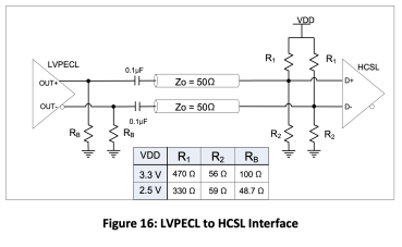
5. Driving an HCSL Receiver with LVPECL Oscillators
A typical HCSL interface utilizes a current mode driver and uses 50Ω-to-GND terminations at the source and no termination at the receiver side. Additionally for an HCSL output driver, an LVPECL driver can be used to drive an HCSL input. Figure 16 shows a recommended termination schematic for driving an HCSL receiver with LVPECL output. To meet the VOH level of 750 mV and VOL level of 0V required by the HCSL receiver, it features AC-coupling capacitors to separate source and load bias voltages.
Thevenin equivalent termination on the load side also sets proper common mode voltage on the receiver inputs. Resistor RB provides proper DC biasing of the LVPECL driver. Recommended termination network component values are indicated in Figure 16 for both 2.5V and 3.3V operation voltages.
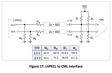
6 Driving a CML Receiver with LVPECL Oscillators
Most SiTime differential oscillators don’t have a CML output option, but they can be used to drive a CML receiver using an LVPECL driver. In this case, the termination schematic has to ensure 400-mV singleended voltage swings at the receiver inputs and VDD – 200 mV common mode voltage [2]. Figure 17 shows a recommended termination schematic for driving a CML receiver with LVPECL output. ACcoupling capacitors for DC current isolation are necessary due to the large difference between LVPECL and CML common mode voltages. Resistor RB is used for proper biasing of the LVPECL driver. Thevenin equivalent termination at the receiver side sets the proper bias voltage and together with RB resistor ensures proper signal swing.
7 Driving Self-Biased Differential Inputs
Many differential receivers have on-chip DC-bias circuits and/or termination networks. In this case, oscillator outputs should be AC-coupled. If external biasing is required, it should be designed according to the datasheet of the receiver device.
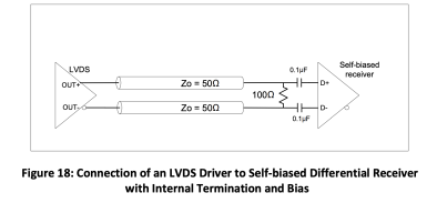
LVDS or LVPECL oscillators may be used to drive self-biased differential inputs. LVDS output requires fewer passive components and lower running power. If 700 mV of LVDS swing is sufficient for the receiver, it is preferable to use an LVDS oscillator. Figure 18 shows interfacing of an LVDS oscillator to a self-biased differential receiver.
LVPECL output can create up to 1.6V differential swing at the receiver. Figure 19 illustrates a schematic for connecting an LVPECL oscillator to a self-biased differential receiver. Resistor RS creates a voltage divider with termination at the load side. Voltage swing on receiver input may be set by selecting the RS value. RB provides DC bias current for the LVPECL driver and its value may be calculated from Equation 1. Please note that the receiver will see an effective termination resistance value of RS + 50Ω.
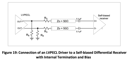
To maintain signal integrity, RS and RB should be placed before the transmission line as close to the oscillator as possible. The load side termination network should be placed as close as possible to the receiver inputs.
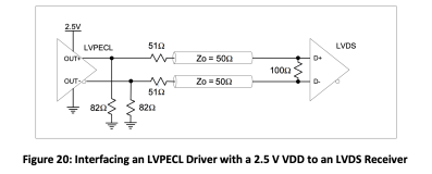
8 Driving an LVDS Receiver with an LVPECL Driver
An LVDS receiver can be driven with an LVPECL clock signal. This requires using termination techniques that puts the signal at the receiver side within the LVDS signaling requirements. Signal common mode voltage and signal amplitude are the main specifications that must be met. To meet LVDS specifications, LVPECL signal amplitude must be reduced from 1.6V to 0.75V. The common mode voltage of the LVPECL driver depends on supply voltage, and for 2.5V VDD it matches the LVDS common mode voltage. Termination that allows clocking an LVDS receiver with a 2.5V LVPECL driver is shown in Figure 20.
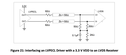
In the case of 3.3V VDD, the common mode voltages of the LVPECL driver and LVDS receiver are different. Figure 21 suggests using series resistors and Y-termination to interface between an LVPECL driver and an LVDS receiver.
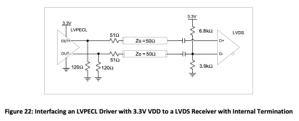
If the receiver has on-chip termination, AC-coupling is recommended as shown in Figure 22. Common mode is set by a resistor divider. Since its equivalent resistance is too high to cause misbalance between positive and negative inputs, only one of the inputs is biased.
9 Interfacing an LVCMOS Oscillator to an LVDS/LVPECL Input
In some cases, clocking differential LVDS or LVPECL receivers with a single-ended output source is needed. LVCMOS output can be interfaced to an LVDS or LVPECL receiver by connecting an AC signal to one of the differential input pins and applying DC threshold voltage to the other pin. To meet differential swing requirements, the amplitude of a single-ended clock at the receiver side must be twice as high as the differential swing of an LVDS or LVPECL interface. Refer to the receiver datasheet to make sure the input voltage is within acceptable limits.
Driving LVDS/LVPECL input with a single-ended oscillator offers much lower power consumption compared to a differential oscillator, but it decreases noise immunity.
Interfacing a single-ended output to a differential receiver requires the following conditions:
1. Common mode voltage at inputs should be 1.2V for LVDS at all VDDs, 1.2V for LVPECL at 2.5V VDD, and 2V for LVPECL at 3.3V VDD.
2. Voltage swing across inputs should be 700 mV to 800 mV for LVDS and 1.2V to 2V for LVPECL.
3. Input impedance of the termination circuit must match trace impedance to maintain signal integrity. Typical trace impedance is 50Ω.
Figure 23 shows a recommended schematic for interfacing single-ended output to any voltage LVDS and LVPECL at 2.5V VDD. Common mode voltage is set by a voltage divider created by output driver impedance and resistors R1 and R3. Capacitor C1 provides an AC-signal path from negative input to ground. Signal amplitude at the positive input is set by the voltage divider, which consists of output driver resistance in series with R1, and R2 in parallel with R3.
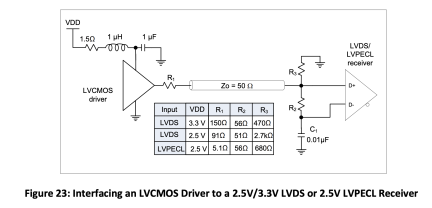
Figure 24 shows a schematic for interfacing LVCMOS to LVPECL at 3.3V VDD. Common mode voltage at the receiver side is set by a voltage divider created by output driver impedance in series with a 27Ω resistor and 200Ω pullup to VDD.
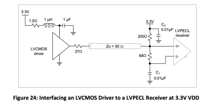
The recommended component values in Figure 23 and Figure 24 are computed based on 25Ω LVCMOS driver impedance. This value corresponds to the typical driver impedance of the SiT8008 family of LVCMOS oscillators.
The LVCMOS oscillator has a RLC filter in its power supply network in Figure 23 and Figure 24. SiTime recommends using this RLC filter since it significantly improves power supply noise rejection.
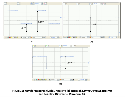
Figure 25 shows examples of waveforms on the inputs of the 3.3V LVPECL receiver when driven with a single-ended clock.
10 Conclusion
This application note presents the output driver structures for SiTime differential oscillators and the most commonly used AC-coupled and DC-coupled termination schemes for LVPECL, LVDS, and HCSL differential outputs. Recommended options for interfacing to HCSL and CML receivers with LVPECL output are discussed. Termination schemes, which allow driving an LVDS or LVPECL clock receiver using a single-ended LVCMOS oscillator, are also presented. With a wide selection of output types, users can select an output signal that best fits their requirements.