SiTime’s MEMS First and EpiSeal Processes
Content
1. Introduction
1.1 Encapsulation
1.2 Stability
1.3 Durability
1.4 Size
1.5 Manufacturability
1.6 Quality
2. Detailed MEMS First Process Flow
2.1 Resonator Definition
2.2 Oxide Fill
2.3 Vent Formation
2.4 Resonator Release
2.5 EpiSeal Resonator Encapsulation
2.6 Via Formation
2.7 Metalization
3. Features and Benefits of the MEMS First Process
4. Conclusion
1. Introduction
MEMS First™ and EpiSeal™ are proprietary processes used by SiTime to manufacture very small silicon resonator die that are fully encapsulated in silicon, extremely stable, and highly durable. Because these processes use standard CMOS foundry tools and materials, they produce products are highly manufacturable with excellent quality and reliability. Moreover, production on a large wafer format results in high volume and fast volume ramping. The following sections explore the key aspects of the MEMS First and EpiSeal processes in more detail.
1.1 Encapsulation
Prior to the development of the MEMS First process, packaging was the foremost problem restraining the commercialization of MEMS resonators. The MEMS First process removes this constraint by producing finished wafers with resonators enclosed within individual micro-vacuum chambers. These wafers look like standard CMOS wafers and can be packaged with industry standard IC packaging processes such as plastic molding, flip chip, chip stack, and chip-scale packaging.
1.2 Stability
The hermetic sealing feature of the MEMS First process, called EpiSeal, is done at very high temperature in a clean vacuum environment. This leads to the high stability of the resonators. Conventional low temperature packaging, that uses ceramic packages or wafer bonding, leaves volatile organics and water residues in the package which cause mass loading of the resonator and frequency drift. MEMS First with EpiSeal is the only demonstrated fabrication process that produces resonators with stability that is comparable to or exceeding quartz crystals.
1.3 Durability
The MEMS First encapsulation is strong and highly robust. The resonators are protected under a layer of silicon that can withstand the high pressure used in plastic molding which can reach 100 bar, or 1500 PSI. The MEMS First encapsulation remains intact at this pressure.
1.4 Size
MEMS First encapsulation requires no additional chip area compared to the other packaging methods such as wafer bonding. Finished MEMS First wafers can be back-grounded to less than 100 um thick. Because of this, SiTime resonators are the world’s smallest and thinnest. In addition, MEMS First encapsulation enables use of advanced IC packaging technology that results in the world’s smallest oscillators.
1.5 Manufacturability
SiTime uses state-of-the-art 200 mm CMOS manufacturing tools and facilities that enable use of a standard supply chain with the benefits of reliability of scheduling, scalability to volume, and economy of production.
1.6 Quality
An outstanding feature of modern CMOS wafer fabrication is the ability to precisely repeat the fabrication steps from wafer to wafer, lot to lot, and year to year with excellent control. SiTime leverages this highly accurate repeatability to produce resonators with optimized quality.
2. Detailed MEMS First Process Flow
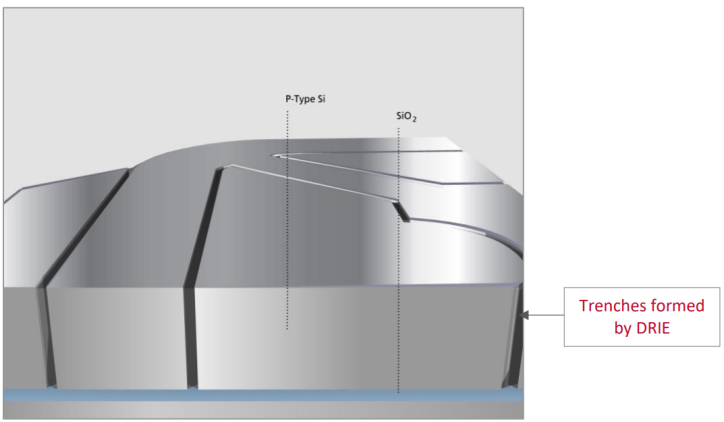
2.1 Resonator Definition
The starting material is a thick silicon on insulator (SOI) wafer. The resonators are formed using the Bosch deep reactive ion etching (DRIE) process.
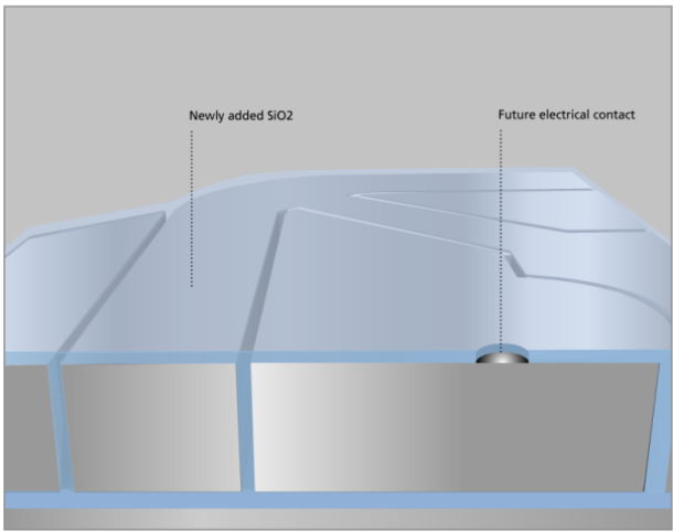
2.2 Oxide Fill
The wafer surfaces are planarized by filling the trenches with oxide and the oxide is patterned to form contact holes. The contact holes are etched to enable electrical connection to the resonator and electrodes. The oxide is also removed from the field areas around the resonators.
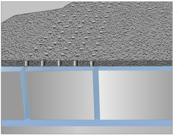
2.3 Vent Formation
Thin silicon layers are grown on top of the oxide, and fine vents are patterned through the layers. The vents enable the removal of the oxide surrounding the resonators, and are positioned above the resonators where they must be free to vibrate.
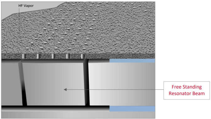
2.4 Resonator Release
The oxide is removed around the resonating structures with hydrofluoric acid (HF) vapor. This step defines the volume of the enclosed vacuum cavities in which the resonators operate. The oxide is not removed where the resonators and electrodes are anchored to the substrates.
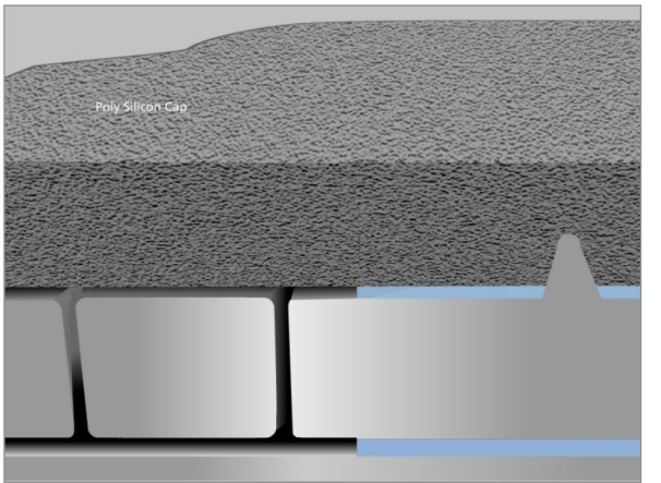
2.5 EpiSeal Resonator Encapsulation
The EpiSeal sealing process is key to forming stable resonators with frequencies that do not drift over time or shift when packaged parts are soldered onto printed circuit boards (PCB). SiTime’s EpiSeal process cleans the resonators and vacuum cavities and then seals the vents closed in high temperature epitaxial reactors. Hot hydrogen and chlorine gas clean the resonators while silicon containing gasses deposit polysilicon in the vents to seal the ultra-clean cavities. After sealing, thick durable encapsulation layers are grown. The chambers surrounding the resonators maintain ultra-clean vacuums.
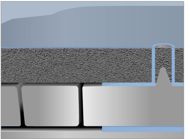
2.6 Via Formation
Electrical vias are made to the resonators and electrodes. Trenches are etched and filled, forming contacts to the electrodes and resonators.
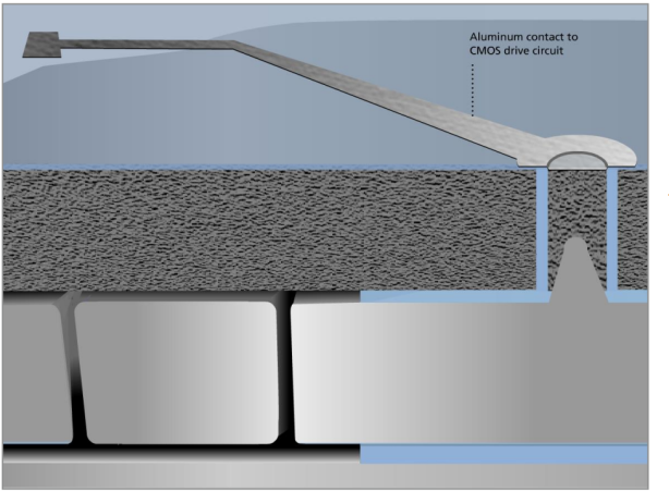
2.7 Metalization
Electrical interconnection is made with aluminum traces and bond pads, and the process is finished with silicon oxide and nitride scratch masks over the traces.
3. Features and Benefits of the MEMS First Process
| Features | Benefits |
|---|---|
| Standard processes and materials | Leverage existing supply chain for lower cost |
| Industry standard process-control and 6-sigma philosophy | Higher yield, quality, and reliability |
| High temperature in-process encapsulation to protect MEMS structure | Smaller size, higher stability, reliability, and quality |
| Standard IC backend (packaging and test) | Leverage existing supply chain for lower cost |
4. Conclusion
SiTime’s MEMS First process with EpiSeal is one of the key technologies that allow SiTime to produce the world’s most advanced, most stable, and most reliable MEMS resonators. This unique patented process is only available from SiTime.